Innoscience Delivers Compact, High-performance ISG3201 SolidGaN Integrated Half-bridge Solution with Driver

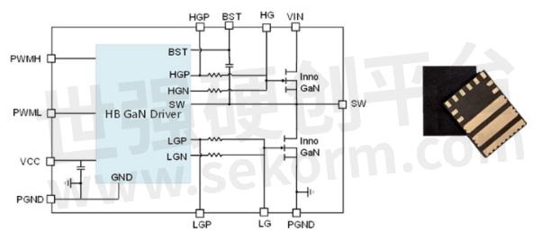
Innoscience Technology, the company founded to create a global energy ecosystem based on high-performance, low-cost, gallium-nitride-on-silicon (GaN-on-Si) power solutions, today launched the first in a new family of SolidGaN integrated GaN devices. ISG3201 is a complete half-bridge circuit including two 100V 3.2mΩ InnoGaN HEMTs and the required driver circuitry in an LGA package measuring just 5x6.5x1.1mm.
Explains Yi Sun, general manager of Innoscience America and Senior VP: “Innoscience is now offering designers a choice between the ultimate flexibility of using a discrete solution, and this new integrated approach which is very compact and simple to use and soldering and simplifying the power stage layout”.
The ISG3201 SolidGaN half-bridge comprises two 100V 3.2mΩ e-mode GaN HEMTs with the driver, driving resistor, bootstrap, and Vcc capacitors. It has a 34A continuous current capability, zero reverse recovery charge, and ultra-low on resistance. Thanks to the high level of integration, gate loop, and power loop parasitics are kept below 1nH. As a result, voltage spikes on switching nodes are minimized. The Turn-On speed of the half-bridge GaN HEMTs can be adjusted using a single resistor.
ISG3201 is suitable for high-frequency Buck converters, half-bridge or full-bridge converters, Class D audio amplifiers, LLC converters, and power modules. Overall, the integrated ISG3201 solution can save up to 20% PCB space on discrete GaN designs and 73% board space on traditional silicon implementations.
Adds Dr. Pengju Kong, VP of Product Design Engineering at Innoscience: “The ISG3201 half-bridge device is the first in a whole family of SolidGaN integrated GaN-based solutions that Innoscience plans to launch this year, including further half-bridge circuits with different voltage ratings. Innoscience aims to offer engineers exactly what they want – integrated solutions or discrete devices – enabling them to achieve the best possible result for their design, minimizing development time and reducing cost.”

- +1 Like
- Add to Favorites
Recommend
- Innoscience to Demonstrate that GaN is The Best Power Solution for An Increasingly Wide Variety of Applications at PCIM 2023
- Innoscience Shipments of InnoGaN Chips Exceed 300 Million Pieces
- Innoscience’s BiGaN technology leads the way toward breakthrough GaN applications for smartphones
- Innoscience Built The First World-class 8-inch Wafer FAB with Gold-free and CMOS Compatible Process
- World‘s Largest Dedicated 8-inch GaN-on-Si FET Producer Innoscience Opens Locations in the USA and Europe Offering Lowest Prices and Wide Availability
- Innoscience‘s Bi-GaN bi-directional GaN HEMTs used inside smartphones save space, increase efficiency and lower temperature rise
- Innoscience Unveils 140W Power Supply Design Using High- and Low-voltage GaN HEMT to Deliver Class-leading Power Density and Efficiency
- Innoscience and University of Bern Develop Multilevel Topology Reference Demo to Address 850VDC Applications With 650V GAN Fulfilling EV and Industrial Requirements
This document is provided by Sekorm Platform for VIP exclusive service. The copyright is owned by Sekorm. Without authorization, any medias, websites or individual are not allowed to reprint. When authorizing the reprint, the link of www.sekorm.com must be indicated.


