Innoscience Built The First World-class 8-inch Wafer FAB with Gold-free and CMOS Compatible Process
Innoscience has a world-leading 8-inch GaN-on-Si industrialization platform, which provides proven capabilities of GaN epitaxial growth, gold-free and CMOS compatible process, as well as reliability testing and failure analysis.
Nanoscience has also established strategic partnerships with top universities, research institutions, and enterprises.
8-Inch GaN-on-Si IDM
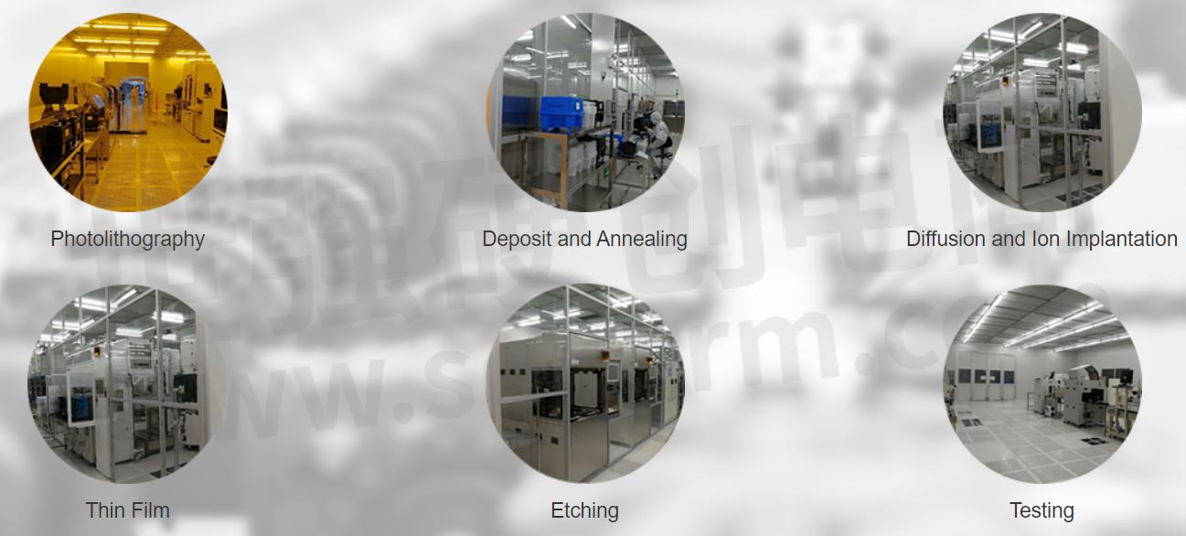
The company built the first world-class 8-inch Wafer FAB in China with gold-free and CMOS compatible processes, including photolithography, thin-film growth, etching, diffusion, testing, and other areas.
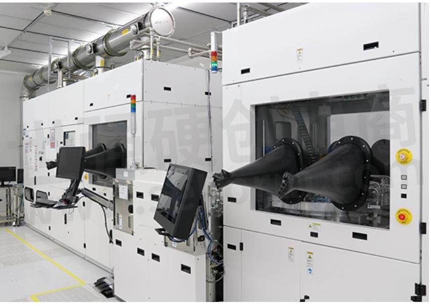
GaN-on-Si Epitaxy
Innoscience owns several world-leading MOCVD equipments for the industrialization of 8-inch GaN-on-Si epitaxy. Through its own patented technology, Innoscience has solved the problems in the 8-inch GaN-on-Si epitaxial growth, including lattice mismatch, thickness uniformity, and thick film growth applied in 650V products.
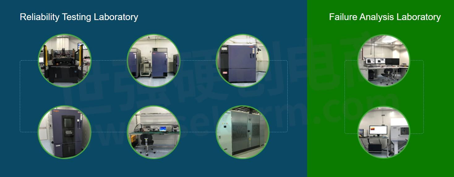
Reliability Testing and Failure Analysis Laboratories
Innoscience owns the industry-leading reliability testing and failure analysis laboratories.
● Reliability Testing Laboratory: It has wafer-level, packaging-level, and system-level testing capabilities. Testing equipment includes Keysight, probe station, HAST, TC, HTGB, HTRB, THB, etc.
● Failure Analysis Laboratory: It has electrical, chemical, and physical analysis capabilities. Analytical equipment includes EMMI/OBIRCH, FIB, high-precision SEM, AFM, grinding machine, etc.
Strategic Partners
Innoscience has established strategic partnerships with research institutions and universities at home and abroad such as Interuniversity Microelectronics Center (IMEC), Hong Kong University of Science and Technology, and University of Electronic Science and Technology to cooperate in the fields of GaN epitaxial growth, manufacture, reliability, and GaN devices as well as an integrated circuit.
For GaN power devices, Innoscience and JCET have jointly developed in the fields of wafer-level packaging, QFN plastic packaging, and chip testing. JCET is the largest packaging and testing enterprise in China.
- +1 Like
- Add to Favorites
Recommend
- World’s Largest 8-inch GaN-on-Si IDM to Debut at Electronica with New Parts, New Demos and Keynote Presentations
- World‘s Largest Dedicated 8-inch GaN-on-Si FET Producer Innoscience Opens Locations in the USA and Europe Offering Lowest Prices and Wide Availability
- Innoscience Shipments of InnoGaN Chips Exceed 300 Million Pieces
- Innoscience Unveils 140W Power Supply Design Using High- and Low-voltage GaN HEMT to Deliver Class-leading Power Density and Efficiency
- Innoscience Delivers 40V Bi-directional GaN HEMT with Ultra-low on Resistance of 7.8mΩ for Mobile Devices, Chargers and Adapters
- Innoscience Demonstrates GaN Leadership at International Symposium on Power Semiconductor Devices (ISPSD) with Two Key Papers
- Inventchip Technology (IVCT) Exhibited SiC and ICs at PCIM Europe | June11-13, 2024
- JieJie Microelectronics launched its 150V SGT MOSFET to Boost Applications in 5G Communication, BLDC, BMS, etc.
This document is provided by Sekorm Platform for VIP exclusive service. The copyright is owned by Sekorm. Without authorization, any medias, websites or individual are not allowed to reprint. When authorizing the reprint, the link of www.sekorm.com must be indicated.
Integrated Circuits


Discrete Components


Connectors & Structural Components


Assembly UnitModules & Accessories


Power Supplies & Power Modules


Electronic Materials


Instrumentation & Test Kit


Electrical Tools & Materials


Mechatronics


Processing & Customization


