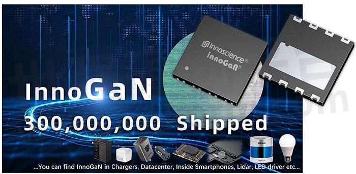
Innoscience Shipments of InnoGaN Chips Exceed 300 Million Pieces
Company increases sales of GaN devices by 500% year-on-year in response to predicted market growth of 65% GAGR 2022-2026
19 September 2023 – Innoscience Technology, the company founded to create a global energy ecosystem based on high-performance, low-cost, gallium-nitride-on-silicon (GaN-on-Si) power solutions, has shipped more than 300 million pieces of its InnoGan gallium nitride chips as of August 2023, helping customers achieve small size, high energy efficiency, and low loss product design.
This is in response to phenomenal market demand across multiple sectors and multiple applications in the consumer category - fast charging, mobile phones, LEDs - as well as automotive LIDAR, data centers, and renewable energy and energy storage systems, which has seen analysts such as TrendForce's in its 2023 GaN Power Semiconductor Market Analysis Report, state that “the global GaN power device market will grow from US$180 million in 2022 to US$1.33 billion in 2026, with compound growth rate of 65%”.
In November 2017, Innoscience began the world's first 8-inch GaN-on-Si mass production line, adopting the Integrated Device Manufacturer (IDM) whole industry chain model, and launched its first low-voltage GaN power device in May 2018. By June 2019, Innoscience's 650V high-voltage GaN device had passed JEDEC approval, and subsequently, Innoscience has been the only semiconductor company in the world that simultaneously mass-produces high-voltage and low-voltage GaN.
Market acceptance of Innoscience’s high quality, high-performance GaN devices has been swift. Following its 2019 entry into the fast charging market, Innoscience’s 650V parts have been adopted in 30W-120W designs by leading brands including ASUS, Anker, Nubia, Baseus, Greenlink, and Flash.
In 2020, Innoscience’s 100V low-voltage GaN was successfully used by Hesai in mass-production LIDAR designs, allowing lasers to achieve image transmission in a shorter time.
In March 2021, the Tencent×Nubia Red Magic mobile phone 6Pro was released. It comes equipped as standard with the industry's first 120W Black Rubik's Cube GaN fast charge, which is based on Innoscience’s 650V chip. With the successive adoption by Oppo, Vivo, Lenovo, and other manufacturers, it has become an industry trend for mobile phones to be equipped with GaN fast charging as standard.
March 2021 saw the mass production of Innoscience's bi-directional conduction chip V-GaN officially begin; this device is the only GaN chip in the world that can be applied to high-voltage side load switches, smartphone USB/wireless charging ports with built-in OVP protection, multi-power supply system switch circuits, and other scenarios: one V-GaN replaces two Si MOSFETs in load switching applications resulting in a smaller and more efficient solution. In October of the same year, Innoscience scored another industry first, as OPPO used the company’s self-developed bi-directional conduction VGaN IC as the internal power switch in its latest smart phone. Other mobile phone makers such as Realme, OnePlus, Lenovo, and Motorola have also successively adopted VGaN for charging protection.
In May 2022, Shounuo released the world's smallest 45W/65W PD car charger, using Innoscience's 40V low-voltage INN040FQ043A.
Then in July, Anker and Innoscience jointly released the world's first 65W full-GaN fast charger. This design uses GaN power chips at both the AC and DC ends for the first time, taking system power density and efficiency to a whole new level.
Later, in October 2022, Innoscience achieved mass production of GaN products targeting industrial power supplies – again an industry first - comprehensively improving energy conversion efficiency and reducing system energy consumption.
In November 2022, Innoscience’s INN100W032A won the IIC World Electronics Achievement Award. The gate charge of this product is only 20% of a traditional silicon MOSFET, and its Ciss is only 40% of its silicon counterpart. It can be widely applied in motor drives, Class D, data centers, motor drivers, communication base stations, and other product fields. In January 2023, Innoscience launched the SolidGaN ISG3201, a 100V highly-integrated half-bridge drive packaged solution, further improving the overall system performance of 48V power supply of data center module power supplies, motor drives, class D power amplifiers, photovoltaic inverters and light hybrid electric vehicles.
The move to GaN as the premium power semiconductor technology is driven both by new GaN products and market demands. As an example, in April this year, Innoscience's IATF 16949 automotive-grade low-voltage parts successfully expanded from industrial to automotive applications, with use in autonomous vehicle LIDAR systems.
Then in July 2023, Innoscience began to apply GaN in the field of renewable energy, reducing the size and improving the efficiency of photovoltaic modules.
By the end of August 2023, Innoscience had successfully mass-produced 54 different types of high-voltage GaN chips (650V-700V) and 20 types of medium-low voltage GaN chips (30V-150V). Products span three chip categories: wafers, discrete devices, and integrated solutions.
Commented Dr Denis Marcon, Innoscience’s General Manager, Europe: “We are just at the start of the GaN story. The first applications were all for consumer, but GaN is undoubtedly the key to reducing costs and increasing efficiency in the industrial field as well. And according to automotive industry forecasts, GaN may enter the automotive market already this year penetrating applications such as low-power OBC and DC-DC applications in 2025. With such rapid growth in market demand, the reliability of devices, price competitiveness, and stable supply in large quantities are now the major concerns of users. Based on an advanced Innoscience’s 8-inch GaN-on-Si IDM manufacturing platform, Innoscience’s current production capacity has reached 15,000 wafers per month, providing tremendous advantages in scale, reliability and cost.”
- +1 Like
- Add to Favorites
Recommend
- Innoscience to Demonstrate that GaN is The Best Power Solution for An Increasingly Wide Variety of Applications at PCIM 2023
- Innoscience’s BiGaN technology leads the way toward breakthrough GaN applications for smartphones
- Innoscience Delivers 40V Bi-directional GaN HEMT with Ultra-low on Resistance of 7.8mΩ for Mobile Devices, Chargers and Adapters
- Innoscience‘s Bi-GaN bi-directional GaN HEMTs used inside smartphones save space, increase efficiency and lower temperature rise
- Innoscience and University of Bern Develop Multilevel Topology Reference Demo to Address 850VDC Applications With 650V GAN Fulfilling EV and Industrial Requirements
- Innoscience Built The First World-class 8-inch Wafer FAB with Gold-free and CMOS Compatible Process
- World‘s Largest Dedicated 8-inch GaN-on-Si FET Producer Innoscience Opens Locations in the USA and Europe Offering Lowest Prices and Wide Availability
- Innoscience Unveils 140W Power Supply Design Using High- and Low-voltage GaN HEMT to Deliver Class-leading Power Density and Efficiency
This document is provided by Sekorm Platform for VIP exclusive service. The copyright is owned by Sekorm. Without authorization, any medias, websites or individual are not allowed to reprint. When authorizing the reprint, the link of www.sekorm.com must be indicated.
Integrated Circuits


Discrete Components


Connectors & Structural Components


Assembly UnitModules & Accessories


Power Supplies & Power Modules


Electronic Materials


Instrumentation & Test Kit


Electrical Tools & Materials


Mechatronics


Processing & Customization


