Innoscience’s BiGaN technology leads the way toward breakthrough GaN applications for smartphones
The UFCS Technical Seminar of the 1st Plug Conference of Guangdong Terminal Fast Charging Industry Association was successfully held on June 28. At the seminar, the Association's Technical Committee and Technical Research Working Group made a detailed introduction to the development trend of fast charging technologies, critical points of UFCS technical standards, and cutting-edge achievements of UFCS technologies.
The plug conference has accelerated the standardization and widespread application of terminal fast charging technologies by bringing together players in the fast charging industry who join hands to promote the research of relevant application scenarios, requirements, technologies, and standards in the fast charging industry.
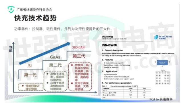
In the plug conference, the father of OPPO VOOC Flash Charge unveiled Innoscience's(英诺赛科) Bi-GaN series for the first time, and the INN40W08 GaN switching tube of the Bi-GaN series also made its appearance.
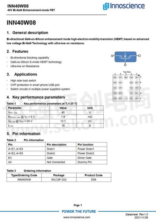
Innoscience INN40W08 is a 40V enhanced small-sized switching tube in the Bi-GaN product family that is packed in a WLCSP 2x2 package. The chip supports bidirectional switching with on-state resistance as low as 7.8mΩ. It can be used in scenarios such as overvoltage protection circuits for smartphone charging, high-side load switching circuits, and switching circuits for multi-power systems.
It is learned that OPPO has already adopted GaN switching tubes in its models with mass production, making it the world's first cell phone manufacturer with built-in GaN charging protection. The technology will also be applied in large quantities in OPPO's future models, which will be a significant move in the industry.
For a long time, silicon MOSFETs have been used in cell phones’ internal power switching devices. However, they not only occupy much space on the motherboard of cell phones but also lead to considerable temperature rise and power loss in case of high power fast charging, which affects the stability and high power duration of fast charging.
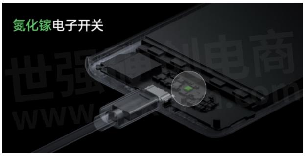
As a third-generation semiconductor material, GaN has superior characteristics such as high frequency, high efficiency, and low resistance, which are vital for efficient charging. In the past, the charging protection was built into the phone charger through GaN power devices. However, with Bi-GaN, GaN chips are now built into the phone.
Thanks to GaN's small resistance per unit length and the fact that it does not have parasitic diodes, one Bi-GaN can be used to replace the previous connected back-to-back NMOS in a common-drain configuration to realize bidirectional switching of a battery's charging and discharging currents, reducing on-state resistance by 50% and temperature rise by 40% in the same board area.
As the charging power of cell phones continues to increase, Innoscience's Bi-GaN series products not only save valuable space inside the phone but also reduce the temperature rise of the phone during charging, maintain a more comfortable temperature during fast charging, extend the duration of fast charging, and provide a better charging experience for users.
It is learned that Innoscience will soon release INN040W048A, the next generation of its BiGaN series, with the same size, 50% reduction in Rds on, and minor conduction loss, making it more competitive in higher power fast charging scenarios. So let's wait and see.
With years of experience in the field of GaN, Innoscience has become the world's leading chip manufacturer and has made breakthroughs in the core technology and critical process of 8-inch GaN-on-Si. Innoscience delivers solutions with internationally advanced performance and has worked with multiple top brands in product and solution design, which customers widely recognize. The application of its Bi-GaN products in the internal power switch of smartphones also marks the arrival of a new era of GaN application.
So far, the application of GaN in the fast charging of consumer goods has been moved to the fast track. In the near future, with its high power density, high frequency, and efficiency features, the application scope of GaN will gradually expand to more fields including new energy vehicles, solar energy, data center, artificial intelligence, and 5G communications, thus becoming an essential part of our everyday life.
- +1 Like
- Add to Favorites
Recommend
This document is provided by Sekorm Platform for VIP exclusive service. The copyright is owned by Sekorm. Without authorization, any medias, websites or individual are not allowed to reprint. When authorizing the reprint, the link of www.sekorm.com must be indicated.
Integrated Circuits


Discrete Components


Connectors & Structural Components


Assembly UnitModules & Accessories


Power Supplies & Power Modules


Electronic Materials


Instrumentation & Test Kit


Electrical Tools & Materials


Mechatronics


Processing & Customization


