World‘s Largest Dedicated 8-inch GaN-on-Si FET Producer Innoscience Opens Locations in the USA and Europe Offering Lowest Prices and Wide Availability
January 18, 2022 –Innoscience Technology, the company founded to create a global energy ecosystem based on high-performance, low-cost Gallium-Nitride-on-Silicon (GaN-on-Si) power solutions, today announced the official launch of its international operations in the USA and Europe. Headquartered in Suzhou, China, Innoscience is now poised to support customers through the addition of design and sales support facilities in Santa Clara, California, and Leuven, Belgium.
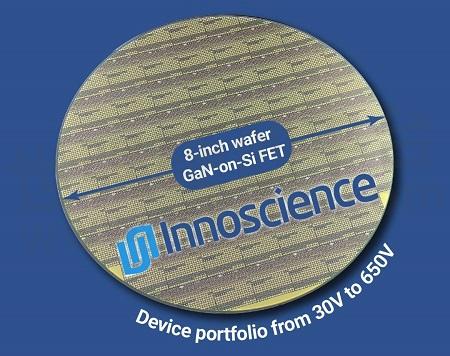
Founded in December 2015, Innoscience is already the largest Integrated Device Manufacturer (IDM) that is fully focused on GaN technology. The company has two wafer fabs including the world's largest dedicated 8-inch GaN-on-Si site, featuring the latest, advanced, high-throughput manufacturing equipment. Currently, the company has a capacity of 10,000 8-inch wafers per month which will ramp up to 14,000 8-inch wafers per month later this year and 70,000 8-inch wafers per month by 2025. The company has a wide portfolio of devices from 30V to 650V and has shipped more than 35 million parts for use in applications including USB PD chargers/adapters, data centers, mobile phones, and LED drivers.
Innoscience produces high-performance, normally off e-mode GaN FETs. By introducing a stress enhancement layer, the company has significantly reduced RDS(on) without affecting other parameters including threshold voltage and leakage. Both epitaxy, as well as device processing, have been optimized to obtain high reproducibility and yield. Parts have passed quality and reliability tests in excess of JEDEC standards.
Comments Dr. Denis Marcon, General Manager, Innoscience Europe: "The time is right for GaN, and Innoscience is ready to supply the world. We will surpass anyone on price for an equivalent device and our huge manufacturing capacity means that our customers are assured of the security of supply, which is often uppermost in people's minds given the shortage of chips at the moment. We look forward to working with any company in order to proliferate GaN throughout the global electronics industry."
Yi Sun, General Manager, Innoscience USA, explained: “This is an exciting time for our customers, who can benefit from Innoscience’s applications understanding and demo boards to develop their unique solutions. This will allow us to better support our customers in the USA, and in particular, the Bay area”.
It is expected both Innoscience offices will expand rapidly in the coming months and years, in order to strategically support Europe’s and the USA’s burgeoning market of GaN-on-Si power solutions.
- +1 Like
- Add to Favorites
Recommend
- EPC GaN FETs Deliver Benchmark Power Density and Efficiency for DC/DC Conversion
- EPC GaN FETs Enable 75 - 231Ampere Laser Diode Control in Nanoseconds for Advanced Automotive Autonomy
- Central Semiconductor Announces New GaN FETs in a Variety of Packages, for Soft Switching Applications with High Efficiency
- How to Design a 2kW 48V/12V Bi-Directional Power Module with GaN FETs for 48V Mild Hybrid Electric Vehicles
- Highest Power Density for Regulated DC-DC Converters Achieved Using EPC GaN FETs and Analog Devices Controller, Efficiency Greater than 96.5 %
- Expanded Family of Packaged GaN FETs Offers Footprint Compatible Solutions to Optimize Performance vs. Cost While Increasing Power Density and Improving Thermal Performance
- EPC and Analog Devices Collaborate to Deliver up to 2MHz Switching Frequency for the Highest Density DC-DC Converters Using GaN FETs
- The 150V, 3mΩ EPC2305 and the 200V, 5mΩ EPC2304 GaN FETs offering higher performance and smaller solution size
This document is provided by Sekorm Platform for VIP exclusive service. The copyright is owned by Sekorm. Without authorization, any medias, websites or individual are not allowed to reprint. When authorizing the reprint, the link of www.sekorm.com must be indicated.
Integrated Circuits


Discrete Components


Connectors & Structural Components


Assembly UnitModules & Accessories


Power Supplies & Power Modules


Electronic Materials


Instrumentation & Test Kit


Electrical Tools & Materials


Mechatronics


Processing & Customization


