Design Higher Power Density USB-C PD Applications with New 50V GaN FET in Tiny 1.8mm² Footprint from EPC

EPC introduces the 50V, 8.5mOhm EPC2057 GaN FET in tiny 1.5mm x 1.2mm footprint, offering higher power density for USB-C PD applications.
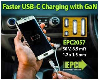
EL SEGUNDO, Calif.— June 2024 — EPC, the world’s leader in enhancement-mode gallium nitride (GaN) power FETs and ICs, launches the 50 V, 8.5 mΩ EPC2057 GaN FET is specifically designed to meet the evolving needs of high-power USB-C devices including those used in consumer electronics, in-car charging, and eMobility.
Key Features and Benefits:
High Efficiency: The new 50 V GaN FET boasts an ultra-low on-resistance of just 8.5 mΩ, significantly reducing power losses and enhancing overall efficiency.
High Efficiency: Its tiny footprint makes it ideal for space-constrained applications, allowing for smaller, more efficient power adapters and chargers.
Fast Switching: The GaN technology enables faster switching speeds, improving power density and reducing the size of passive components, leading to more compact and lightweight designs.
“As USB-C PD continues to gain traction, efficient, compact, high-performance power solutions are vital. Our new GaN FET meets these needs with a reliable, efficient solution that enhances performance,” said Alex Lidow, EPC CEO and co-founder.
Industry Impact
With the increasing adoption of USB-C PD, there is a growing demand for power components that can deliver higher efficiency and performance while minimizing size and heat generation. EPC’s new GaN FET is designed to meet this demand, offering a superior alternative to traditional silicon-based FETs.
The EPC90155 development board is a half bridge featuring the EPC2057 GaN FET. It is designed for 40V maximum operating voltage and 10A maximum output current. The purpose of this board is to simplify the evaluation process of power systems designers to speed their product’s time to market. This 2” x 2” (50.8 mm x 50.8 mm) board is designed for optimal switching performance and contains all critical components for easy evaluation.
- +1 Like
- Add to Favorites
Recommend
- Sharge Selects GaN FETs EPC2218 from EPC for High-power USB PD Charger Retro 67 to Achieve the Most Efficient Power Conversion
- EPC Introduces The 40 V, 1.6 Milliohm EPC2069 EGaN® FET, it Can Range From 500 W to 2 KW and Exceed 98% Efficiency
- EPC Announces a New 3-phase BLDC Motor Drive Inverter Using the EPC2065 EGaN® FET
- EPC Launches 40V EPC2055 eGaN FET Ideal for High Power Density Solutions for USB-C Battery Chargers and Ultra-thin Point-of-Load Converters
- New Automotive Qualified GaN FETs EPC2204A and EPC2218A for Vehicle Electronics and Advanced Autonomy from EPC
- Efficient Power Conversion (EPC) Expands 100 V eGaN FET Family Offering Designers Best-in-Class Performance and Cost for 48 V DC-DC Conversion
- Design Higher Resolution Lidar Systems with New Automotive-Qualified GaN FET EPC2252 for Advanced Autonomy from EPC
- 65A ePower™ Chipset from Efficient Power Conversion (EPC) Redefines Power Conversion
This document is provided by Sekorm Platform for VIP exclusive service. The copyright is owned by Sekorm. Without authorization, any medias, websites or individual are not allowed to reprint. When authorizing the reprint, the link of www.sekorm.com must be indicated.
Integrated Circuits


Discrete Components


Connectors & Structural Components


Assembly UnitModules & Accessories


Power Supplies & Power Modules


Electronic Materials


Instrumentation & Test Kit


Electrical Tools & Materials


Mechatronics


Processing & Customization


