Two kinds of structure of unit in SiC power MOSFET: plane structure and groove structure

There are mainly two kinds of structure of unit in SiC power MOSFET: plane structure and groove structure. The structure of the planar SiC MOSFET is shown in figure 1. This structure is characterized by a simple process, good unit consistency, and high avalanche energy.
However, in the middle of this structure, the N region is sandwiched between two P regions, and when the current is limited to the narrow N region near the P body, the JFET effect will be produced, thus increasing the on-state resistance. at the same time, the parasitic capacitance of this structure is also larger.

Figure 1: the structure of a planar SiC MOSFET.
The structure of the slot SiC MOSFET is shown in figure 2.
In this structure, the gate is embedded in the matrix to form a vertical channel. Due to the trenching, the process becomes complex, and the consistency of the element and the avalanche energy is worse than the plane structure.
However, because this structure can increase the cell density, there is no JFET effect, the channel crystal plane achieves the best channel mobility, and the on-resistance is obviously lower than that of the planar structure; at the same time, the parasitic capacitance is smaller, the switching speed is faster, and the switching loss is very low, so this structure is studied and adopted in the new generation of structures.

Figure 2: structure of trench SiC MOSFET.
The main problem of the groove structure SiC MOSFET is that because the device works in a high voltage state, the internal working electric field strength is high, especially at the bottom of the groove, the working electric field strength is very high, and it is easy to exceed the maximum critical electric field strength locally, resulting in local breakdown and affecting the reliability of the device, as shown in figure 3.

Figure 3: internal working electric field of trench SiC MOSFET structure.
Cymbal. Therefore, the technical evolution direction of the new generation of SiC MOSFET trench structure is how to reduce the working electric field intensity at the bottom of the trench, such as the double trench structure of Rohm, the asymmetric trench structure of Infineon, and so on, as shown in figure 4 and figure 5.
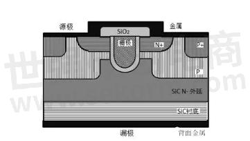
Figure 4:Rohm double trench structure
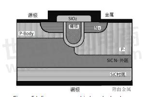
Figure 5:Infineon asymmetric trench structure.
The core of these structures is to either add a buffer layer at the bottom of the groove or move the P region down to form a depletion layer between P and N at the bottom of the groove, as shown in figures 6 and 7 so that the electric field of the oxide layer at the bottom of the groove is partially transferred to the P region depletion layer to reduce the electric field at the bottom of the groove.

Figure 6: Schematic diagram of reducing the working electric field at the bottom of the groove

Figure 7:Infineon asymmetrical groove structure internal electric field distribution (picture source network).
The basic process and cost proportion of planar structure SiC MOSFET is shown in figure 8 and figure 9.
It can be seen that at present, the substrate of SiC crystal still accounts for a very large proportion, reaching 38%. If the substrate thinning and polishing process of SiC crystal is added, the proportion is as high as 50%.
The main reason is that SiC grows slowly, the temperature is high, the process is complex, and it is easy to produce all kinds of lattice defects.
The growth rate of Si is 100mm/hour, the maximum diameter is 450mm, and the maximum thickness is 2m. The growth rate of sic is 100300 um/ hours, 2100 °C, the maximum diameter 150mm, and the maximum thickness 50mm.
The proportion of the cost of the epitaxial process is about 17%, the proportion of the packaging cost is about 11%, and the cost caused by the yield of the product is 21%.
How to control the defects in the SiC MOSFET production process and improve the yield in the production process is still an important problem that manufacturers need to face, which is not only related to the cost of the product but also related to the reliability of the product application in the customer.
Figure 8: basic process of planar structure SiC MOSFET
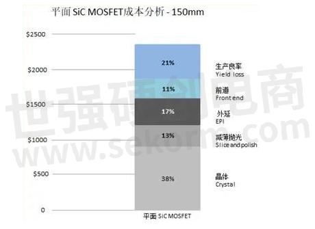
Figure 9: Proportion of process cost of planar structure SiC MOSFET
- +1 Like
- Add to Favorites
Recommend
- 650V Enhancement-mode SiC MOSFET Provides Qoss Almost 1/10 of Advanced Silicon Super-junction MOSFET
- 需要充电吗?具有开尔文源引脚的SiC MOSFET DIF120SIC053-AQ加速电动汽车充电过程
- Vincotech’s 70A flowPACK 1 SiC Modules Featuring Ultra-fast 900V SiC MOSFET for up to 400kHz switching frequency
- SiC MOSFETs and SiC Schottky Diodes in TO-247-3L&4L for Sustainable Public Transportation
- Ultra-Low On-Resistance 1200V/7mΩ SiC MOSFET N2M120007PP0 Launched by NEXIC for Renewable Energy Applications
- Achieve Zero Switching Loss with SiC MOSFET
- Littelfuse Unveils Industry’s First Asymmetrical TVS Diode Series for SiC MOSFET Gate Protection
- Littelfuse IX4351NE SiC MOSFET & IGBT Driver Wins Annual Power Product Award
This document is provided by Sekorm Platform for VIP exclusive service. The copyright is owned by Sekorm. Without authorization, any medias, websites or individual are not allowed to reprint. When authorizing the reprint, the link of www.sekorm.com must be indicated.
Integrated Circuits


Discrete Components


Connectors & Structural Components


Assembly UnitModules & Accessories


Power Supplies & Power Modules


Electronic Materials


Instrumentation & Test Kit


Electrical Tools & Materials


Mechatronics


Processing & Customization


