EPC2152 GaN Integrated Power Stage – Redefining Power Conversion

Integrated circuits made using GaN-on-Si substrates have been in production for over five years. Since that time, GaN-based ICs have gone through various “phases” of integration from pure discrete devices to monolithic half-bridge devices, to power FETs that included their own monolithically integrated driver, and more recently, to fully monolithic power stages containing power FETs, drivers, level shifting circuits, logic, and protection.
Phase One Integration – Monolithic Half Bridges
The most common building block used in power conversion is the half bridge. Half bridges are used in buck converters, boost converters, LLC converters, bus converters, motor drives, and many more converter topologies. Therefore, in September 2014, the first step towards a power system integrated onto one semiconductor substrate was taken when the monolithic half bridge was introduced. The first of these devices, shown in figure 1 (a), put both the high-side and low-side transistors onto one substrate. The circuit equivalent of this half bridge is shown in figure 1 (b). The advantages of this integration included the reduction in size and cost, and by virtue of the close coupling of the two transistors, the parasitic common source inductances were also reduced. This last advantage increased switching speed and therefore enabled even faster switching power conversion systems.
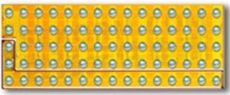
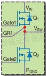
Figure 1: (a) Image of an EPC2100 monolithic half bridge measuring 6 mm × 2 mm, and (b) equivalent circuit diagram
This was a good first step, however users of GaN transistors or GaN half-bridge devices still had to add their own driver circuits. Texas Instruments, Silicon Labs, μPI Semiconductor, Murata Semiconductor, and several others introduced driver ICs made with traditional silicon processes that could easily interface with enhancement mode GaN transistors. Unfortunately, the added size, and cost, as well as the added parasitic gate loop inductance of these drivers detracted from the ultimate potential for GaN in a power conversion system.
Phase Two Integration – Half Bridge Plus Driver
To address the issue of external gate drivers, early in 2018 devices that added the driver onto the GaN transistor arrived with the device shown in figure 2 (a), with the equivalent circuit shown in figure 2 (b). In GaN, low voltage transistors can be fabricated with very short gatedrain separation alongside the 200 V power transistors. These GaN FET-plus-driver integrated circuits could be driven at multi-megahertz frequencies from simple CMOS logic, thus eliminating the need for a silicon driver IC.
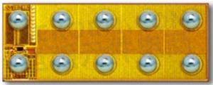
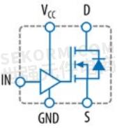
Figure 2: (a) Image of an EPC2112 monolithic GaN-on-Si FET with integrated driver measuring 1.1 mm × 2.9 mm, and (b) equivalent circuit diagram
Phase Three Integration – ePower™ Stage
In early 2019 the driver function and the monolithic half bridge were merged onto a single GaN-on-Si substrate along with a level shifter, synchronous boost circuit, protection and input logic as shown in figures 3 (a) and 3 (b). This complete power stage, the ePower™ Stage, can be driven at multi-megahertz frequencies and controlled by a simple ground-referenced CMOS IC, and with just a few added passive components, could become a complete DC-DC regulator. Figure 4 shows the efficiency of this monolithic power stage at 1 MHz and at 2.5 MHz in a 48 VIN – 12 VOUT buck converter.
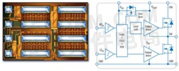
Figure 3: (a) Image of an EPC2152 monolithic ePower Stage measuring 3.9 mm × 2.6 mm, and (b) equivalent circuit diagram
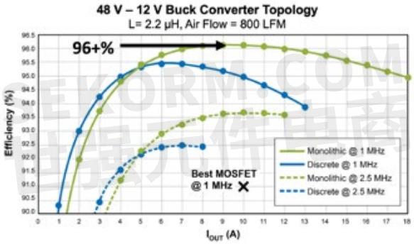
Figure 4: Efficiency vs. output current for a 48 VIN – 12 VOUT buck converter at both 1 MHz and at 2.5 MHz using the EPC2152 monolithic ePower Stage IC compared with the performance of the same circuit using discrete GaN transistors with a silicon half-bridge driver IC.
Figure 5 shows the basic cross-section of this ePower Stage IC. The two power FETs that form the high and low-side of the power stage are accompanied by low-voltage transistors. The level shift transistor on the far left must have the same voltage rating as the output FETs, but the signal-level devices used for driver and logic functions can have a lower voltage capability, and therefore a much smaller separation between gate and drain electrodes. Not shown in this diagram are the numerous capacitors and resistors that complete the circuit.
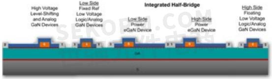
Figure 5: Cross section of a monolithic power stage showing highside and low-side power devices with their accompanying low voltage driver and level shift devices
The ePower™ Stage replaces at least three discrete chips; the gate driver plus two FETs making design and manufacturing easier. The device saves at least 33% of space on the printed circuit board compared to a discrete implementation as seen in figure 6. This device makes it easy for designers to take advantage of the significant performance improvements made possible with GaN technology. Integrated devices in a single chip are easier to design, easier to layout, easier to assemble, save space on the PCB, and increase efficiency.
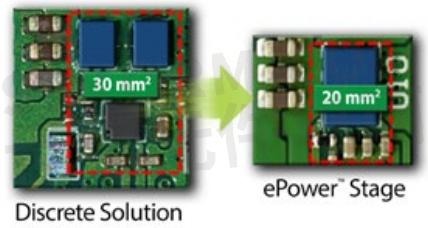
Figure 6: Comparison of discrete implementation of power stage for 48 V – 12 V buck converter vs. monolithic ePower™ Stage implementation. Integration provides 33% space savings on the PCB.
The Future
The monolithic power stage IC discussed in the previous section performs all the same basic functions as a multi-chip DrMOS module based on silicon MOSFETs, but at higher voltages, higher switching speed, lower cost, and in a smaller footprint. This, however, is only the beginning of the integration opportunities for GaNon-Si devices. These first-generation power stages only include capacitors, resistors and lateral n-channel FETs. Soon additional sensing of current and temperature can be added, along with circuit blocks such as references, comparators and op amps to construct an integrated controller plus output stage on a single chip. Multilevel topologies can also be integrated, thus enabling higher input voltages with lower voltage power devices.
Eventually p-channel devices will also be monolithically integrated based on one of the many hopeful structures now in development. Once complimentary n- and p-channel devices can be integrated, CMOS circuitry will be possible, thus enabling more efficient driver and logic circuits.
By going to very high frequencies – above 30 MHz – the size of passive components become so small that it will be possible to integrate all the components needed for a full power supply converter on a single chip. This will all happen, it’s just a question of time!
- 氮化镓技术综述
- 【Datasheet】EPC2100 – Enhancement-Mode GaN Power Transistor Half-Bridge V-DS,30 V R-DS(on),8.2 mΩ (Q1),2.1 mΩ (Q2) I-D,10A (Q1),40A (Q2) DATASHEET
- Material Composition Declaration
- 【Datasheet】EPC2100 – Enhancement-Mode GaN Power Transistor Half-Bridge
- 利用单片氮化镓电源设计小型低压无刷直流电机驱动逆变器™ 舞台
- How2应用020如何使用单片氮化镓ePower设计双向1/16砖48 V-12 V转换器™ 舞台
- 如何使用单片氮化镓ePower设计小型低压无刷直流电机驱动逆变器应用说明
- EPC2100 Material Composition Declaration
- 【Datasheet】EPC2100 – Enhancement-Mode GaN Power Transistor Half-Bridge DATA SHEET
- 【Datasheet】EPC2100 – Enhancement Mode GaN Power Transistor Half Bridge Preliminary Specification Sheet
- 【Datasheet】EPC2152 80 V, 15 A ePower™ Stage Preliminary Datasheet
- 【Datasheet】EPC2152 80 V, 15 A ePower™ Stage Preliminary Datasheet
- +1 Like
- Add to Favorites
Recommend
This document is provided by Sekorm Platform for VIP exclusive service. The copyright is owned by Sekorm. Without authorization, any medias, websites or individual are not allowed to reprint. When authorizing the reprint, the link of www.sekorm.com must be indicated.
Integrated Circuits


Discrete Components


Connectors & Structural Components


Assembly UnitModules & Accessories


Power Supplies & Power Modules


Electronic Materials


Instrumentation & Test Kit


Electrical Tools & Materials


Mechatronics


Processing & Customization


