Explain in Detail the Cause of MOS Tube Heating

For power supply design or driving circuits, it is inevitable to use a field effect tube, which is often called an MOS tube. There are many kinds of MOS tubes and they have many functions. To do the use of power or drive, of course, is to use its switching action.
Regardless of N type MOS tube or P type MOS tube, the operating principle is essentially the same. MOS transistors control the drain current at the output end by applying a voltage to the gate at the input end. MOS tube is a voltage control device. It controls the characteristics of the device by adding voltage to the grid, which will not cause the charge storage effect caused by the base current when the triode is switched. Therefore, in switching applications, the switching speed of the MOS tube should be faster than that of the triode. Its main principles are as follows:
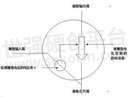
Fig.1
How the MOS tube works
The open-drain circuit of the MOS tube is commonly used in switching the power supply. As shown in FIG. 2, the open-drain is connected to the load intact, which is called an open-drain circuit. No matter how high the load voltage is connected to the open-drain circuit, the load current can be switched on and off. It is an ideal analog switching device. This is the principle of MOS transistors as switching devices. Of course, there are many circuit forms used for MOS tube switches.
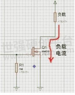
Fig.2 Open drain circuit of NMOS tube
In switching power applications, such applications require MOS tubes to be regularly switched on and off. For example, the basic step-down converters commonly used in DC-DC power supplies rely on two MOS transistors to perform the switching function. These switches alternately store energy in the inductor and release it to the load. We often choose frequencies of hundreds of kHz or even more than 1 MHz, because the higher the frequency, magnetic elements can be smaller and lighter. During normal operation, the MOS tube is only equivalent to a conductor. Therefore, what we circuit or power supply designers are most concerned with is the minimum conduction loss of MOS.
MOS tube manufacturers use RDS(ON) parameters to define the on-off impedance. For switching applications, RDS(ON) is also the most important device feature. The data sheet defines RDS(ON) as relating to the gate (or drive) voltage VGS and the current flowing through the switch, but for a full gate drive, RDS(ON) is a relatively static parameter. MOS tubes that are always on are easily heated. In addition, a slowly rising junction temperature will also lead to an increase in RDS(ON). The MOS tube data sheet specifies the thermal impedance parameters, which are defined as the semiconductor junction heat dissipation capability of the MOS tube package. The simplest definition of RθJC is the thermal impedance to the shell.
1. In the heating situation, the circuit design problem is to make the MOS tube work in the linear working state, rather than in the switching state. This is also a cause of MOS tube heating. If N-MOS is used as a switch, the G voltage must be several V higher than the power supply to fully conduct, while p-MOS is the opposite. The power consumption is caused by the high-pressure drop due to the incomplete opening. The equivalent DC impedance is relatively large, and the pressure drop increases. Therefore, U*I also increases, and the loss means the heating. This is the most taboo mistake in designing a circuit.
2. The frequency is too high, mainly because the excessive pursuit of volume sometimes leads to the increase of frequency, and the loss on the MOS tube increases, so the heating also increases
3. Insufficient heat dissipation design, too high current, MOS tube nominal current value, generally need good heat dissipation to achieve. Therefore, ID is less than the maximum current, and the heat may be severe, so sufficient auxiliary heat sinks are needed.
4. Wrong selection of MOS tube, wrong judgment on power, insufficient consideration of internal resistance of MOS tube, resulting in increased switching impedance.
- +1 Like
- Add to Favorites
Recommend
- Details of MOS tube packaging
- The Differences between MOS Tube and IGBT Tube
- MOS Tube Drive Circuit Summary - Detailed Design of Various Switching Power Supply MOS Tube Drive Circuit
- What is the Difference between MOS tube and IGBT?
- MOS Tube Knowledge, Must Read!
- How to Judge the Working State of MOS Tube?
- MOS Tube Anti-overvoltage Circuit
- Analysis of Classic MOS Tube Drive Circuit
This document is provided by Sekorm Platform for VIP exclusive service. The copyright is owned by Sekorm. Without authorization, any medias, websites or individual are not allowed to reprint. When authorizing the reprint, the link of www.sekorm.com must be indicated.
Integrated Circuits


Discrete Components


Connectors & Structural Components


Assembly UnitModules & Accessories


Power Supplies & Power Modules


Electronic Materials


Instrumentation & Test Kit


Electrical Tools & Materials


Mechatronics


Processing & Customization


