MOS Tube Knowledge, Must Read!

The MOS tube is briefly summarized in this paper. The following is the directory of this paper:
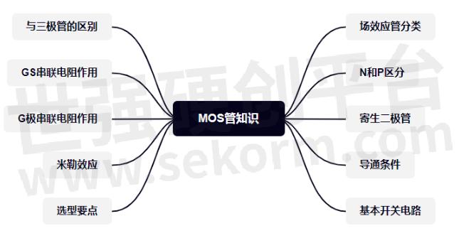
Fig.1
Field effect tube classification
There are two types of JFET and MOSFET.
The full English name of JFET -- Junction field-effect supply be visualized in either the N channel or P channel, which is virtually non-existent in reality.
The MOSFET is the metal-oxide -Semiconductor field-effect Transistor. It is widely used as a MOS Transistor.
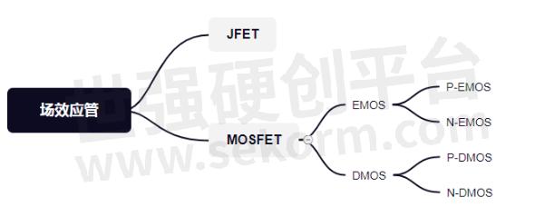
Fig.2
MOSFET can be divided into two categories: enhanced type and depleted type. Under each category are NMOS and PMOS.
The English word for the enhanced MOS tube is Enhancement MOS or EMOS, while the English word for the depleted MOS tube is Depletion MOS or DMOS.
The most commonly used motherboard is an enhanced MOS tube, NMOS is most commonly used in signal control, followed by PMOS, mostly used in power switches and other aspects, with almost no depletion type.
N and P
The following red arrow pointing to the G pole is NMOS, while the arrow pointing back to the G pole is PMOS.
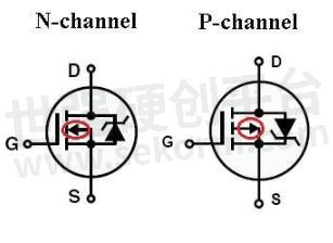
Fig.3
As can be seen from the figure above, the direction of NMOS and PMOS parasitic diodes is different. NMOS →D pole, while PMOS →S pole.
The parasitic diode is the same as the ordinary diode, the positive connection will lead and the reverse connection will cut off. For NMOS, when the S pole is connected to the positive, and the D pole to the negative, the parasitic diode will lead on, and vice versa. For the PMOS tube, when the D pole is connected to the positive, the S pole to the negative, parasitic diode conduction, and vice versa.
In some applications, stripper diodes are also selected to reduce the voltage drop between DS (the voltage drop of the bulk diodes is much larger than the on-off voltage drop of the MOS), as well as the over-current capability of the bulk diodes.
When meeting the MOS tube conduction condition, the D and S pole of MOS tube conduction, this time the body diode is by the state, because of the MOS tube conduction resistance tiny, general m Ω level, through the current of 1 a level, just also mV level, so the D and S pole conduction between the pressure drop is small, enough to reduce parasitic diode conduction, which needs special attention.
Conduction condition
MOS tube is a pressure-controlled type, and its conduction is determined by the pressure difference between G and S poles.
For NMOS, VG-VS >VGS(TH), i.e., the pressure difference between the G pole and the S pole is greater than a certain value, the MOS tube will conduct conduction, but it should not be too large, otherwise, the MOS tube will be burned out. The opening voltage and other parameters can be determined by the SPEC of the specific device.
For PMOS, VG-VS >VGS(TH), that is, the pressure difference between the S pole and the G pole is greater than a certain value, and the MOS tube will conduct. Similarly, the specific parameters depend on the SPEC of the device.
Basic switching circuit
NMOS switch circuit
When the GPIO_CTRL voltage is less than the MOS tube opening voltage, the MOS tube stops, and OUT is pulled up to 5V through R1, and OUT=5V.
When the GPIO_CTRL voltage is greater than the MOS tube opening voltage, the MOS tube is on, and the D-pole voltage is equal to the S-pole voltage, that is, OUT=0V.
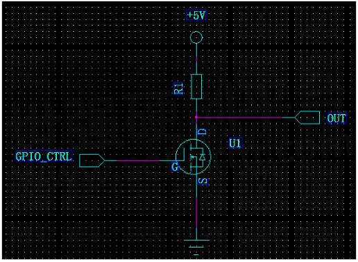
Fig.4
PMOS switch circuit
PMOS tube is most commonly used in power switching circuits. As shown in the following figure, when GPIO_CRTL=0V, the differential pressure between S and G is greater than the MOS tube opening voltage, MOS tube conducting, 5V_VOUT=5V_VIN.
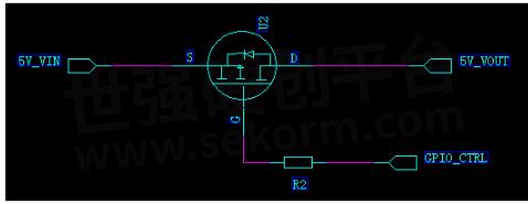
Fig.5
The difference with a triode
Triode is the current control, and MOS tube is the voltage control, there are mainly the following differences:
1. Choose an MOS tube when only a small amount of current is allowed from the signal source; Under the condition of low signal voltage and allowing more current to be taken from the signal source, a triode is selected.
2. The MOS tube is a unipolar device (conducting by a majority of carriers), and the audion is a bipolar device (conducting by both majority and minority carriers).
3. The source and drain of some MOS tubes can be used interchangeably, and the gate can be positive or negative, which is more flexible than the triode.
4. MOS tubes are widely used and can operate at very low current and voltage.
5, MOS tube input impedance is large, low noise, MOS tube is more expensive, the transistor loss is large.
6, MOS tube is commonly used as a power switch, as well as large current switching circuit, high frequency high-speed circuit, triode is commonly used for digital circuit switch control.
The effect of the series resistance of G and S poles
The MOS tube is a voltage-controlled type. In some cases, why do we need a resistor in series at the G pole?
1, slow down RDS from infinity to RDS(ON).
2. Avoid shock. Generally, the I/O output of the single chip microcomputer will have some stray inductance. In the case of voltage mutation, LC shock may be formed with the grid capacitance.
3. Reduce the peak current of gate charging.
Miller effect of MOS tube
About the Miller effect of MOS tube, you can read the article:http://www.HI-SEMICON.com/info-detail/id-27.html
Selection of the main points
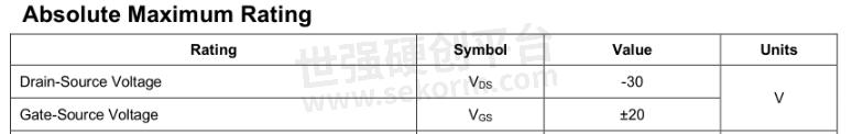
1. The voltage value
Pay attention to the maximum VDS on-off voltage and the maximum VGS withstand voltage. In actual use, the value should not be exceeded, otherwise the MOS tube will be damaged.
Table.1
Pay attention to on voltage VGS(TH). Generally, MOS transistors are controlled by single-chip microcomputer. According to the level of GPIO of a single-chip microcomputer, MOS transistors with appropriate conduction threshold are selected, and a certain margin is left as far as possible to ensure that MOS can be switched normally.
Table.2
![]()
2. The current value
Pay attention to ID current. This value represents how much current can flow through the PMOS tube and reflects its ability to carry a load. Beyond this value, the MOS tube will also be damaged.
Table.3

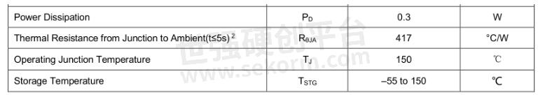
3. Power loss
Power loss needs to be concerned with the following parameters, including thermal resistance and temperature. Thermal resistance refers to the ratio between the temperature difference at both ends of the object and the power of the heat source when heat is transmitted over the object. The unit of thermal resistance is ℃/W or K/W. The formula of thermal resistance is ThetaJA = (TJ-TA)/P, which is related to both power and ambient temperature.
Table.4
4. Conduction of internal resistance
Conduction resistance ON PMOS RDS (ON) parameters, the smaller the conduction resistance, the smaller the wastage of the PMOS tube, PMOS tube conduction resistance is in commonly m Ω level.
5. Switching time
MOS as a switching device, there will be the concept of switching time, in the high-speed circuit, as far as possible to choose the input and output capacitance CISS&COSS small, switch time Ton&Toff short MOS tube, to ensure normal data communication.
6. Packaging
According to the size of the PCB board, select the appropriate PMOS tube size, in the case of limited onboard area, choose the small package as far as possible; As far as possible select common packaging, to prepare for the subsequent selection of appropriate replacement material.
- +1 Like
- Add to Favorites
Recommend
- Details of MOS tube packaging
- The Differences between MOS Tube and IGBT Tube
- MOS Tube Drive Circuit Summary - Detailed Design of Various Switching Power Supply MOS Tube Drive Circuit
- Explain in Detail the Cause of MOS Tube Heating
- What is the Difference between MOS tube and IGBT?
- How to Judge the Working State of MOS Tube?
- MOS Tube Anti-overvoltage Circuit
- Analysis of Classic MOS Tube Drive Circuit
This document is provided by Sekorm Platform for VIP exclusive service. The copyright is owned by Sekorm. Without authorization, any medias, websites or individual are not allowed to reprint. When authorizing the reprint, the link of www.sekorm.com must be indicated.
Integrated Circuits


Discrete Components


Connectors & Structural Components


Assembly UnitModules & Accessories


Power Supplies & Power Modules


Electronic Materials


Instrumentation & Test Kit


Electrical Tools & Materials


Mechatronics


Processing & Customization


