MOS Tube Drive Circuit Summary - Detailed Design of Various Switching Power Supply MOS Tube Drive Circuit

MOS tube drive circuit design
When using an MOS tube drive circuit to design a switch power supply or motor drive circuit, most people will consider MOS conduction resistance, maximum voltage, maximum current, etc., and many people only consider these factors. Such circuits may work, but they are not excellent and are not allowed as a formal product design.
1. MOS type and structure
MOS tube is one kind of FET (the other is JFET), which can be manufactured into enhanced or exhausted types. There are four types of P channel or N channel but only enhanced N channel MOS tube and enhanced P channel MOS tube are used in practice. Therefore, NMOS is usually mentioned, or PMOS refers to these two types. On the right is the symbol for the two MOS tubes.
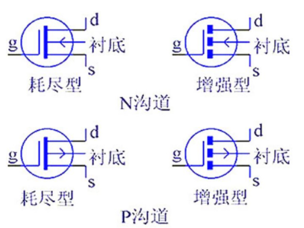
Fig.1
As to why not use a depletion-type MOS tube, it is not recommended to ask. For these two kinds of enhanced MOS tubes, NMOS is more commonly used. The reason is that the conduction resistance is small and easy to manufacture. Therefore, NMOS is commonly used in switching power supply and motor drive applications. In the following introduction, also mostly with NMOS.
As can be seen in the MOS schematic, there is a parasitic diode between the drain and the source. This is called a volume diode, which is important in driving inductive loads such as motors. It exists in a single MOS tube but is usually not found inside an IC chip. The following is the construction diagram of the MOS tube, which is usually drawn as shown in the schematic diagram on the right.
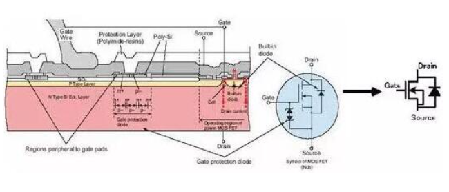
Fig.2
There is parasitic capacitance between the three pins of the MOS tube, as shown in the figure on the right. This is not what we need, but is due to manufacturing process constraints. The existence of parasitic capacitance makes it more difficult to design or select the drive circuit, but there is no way to avoid, it MOS tube drive circuit design will be introduced in detail.
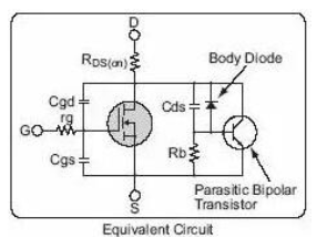
Fig.3
2. Conduction characteristics of MOS tube
reaches 4V and the pressure drop between DS is already very small, so the conduction can be considered.VGS voltage diagram of renesas 2SK3418. It can be seen that when the current is small, the VDS voltage and VGSOn the right is the V connected to the situation (high-end driver). However, although PMOS can be easily used as high-end drivers, NMOS is usually still used in high-end drivers due to its high on-off resistance, high price, and few replacement types.CC less than a certain value will be on, using the source VGSPMOS characteristics, V is greater than a certain value, it will conduct. It is suitable for the situation when the source is grounded (low-end drive), as long as the gate voltage reaches 4V or 10V.GSNMOS features that when the V To conduct means to act as a switch, equivalent to a switch being closed.
Fig.4
3. MOS switch tube loss
The figure below shows the waveforms of MOS tube conduction. It can be seen that the product of voltage and current at the moment of conduction is very large, resulting in a great loss. Reducing the switching time can reduce the loss of each conduction. Reducing the switching frequency can reduce the number of switches per unit of time. Both methods can reduce switch loss.
MOS must not be done instantaneously when conducting and cutting off. The voltage at both ends of MOS has a descending process, while the current flowing through it has a rising process. During this period, the loss of the MOS tube is the product of voltage and current, which is called switch loss. Generally, the switch loss is much greater than the on-off loss, and the faster the switch frequency, the greater the loss.
Whether it is NMOS or PMOS, there is a conduction resistance after the conduction, so when the current flows between DS, there is also a voltage at both ends (as shown in the 2SK3418 characteristic diagram), so the current will consume energy on this resistance, and this part of the energy is called the conduction loss. Choosing an MOS tube with small conduction resistance will reduce conduction loss. The current small-power MOS tube conduction resistance is generally in the tens of milliohms, a few milliohms are also available.
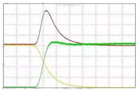
Fig.5
4. MOS tube drive
Compared with bipolar transistors, it is generally believed that MOS tube conduction does not require current, as long as the GS voltage is higher than a certain value, it is ok. That's easy to do, but we also need speed.
In the structure of the MOS tube, it can be seen that there are parasitic capacitors between GS and GD, while the drive of the MOS tube is the charge and discharge of the capacitor. A current is needed to charge the capacitor because the capacitor can be regarded as a short circuit at the moment of charging, so the instantaneous current will be relatively large. The first thing to note when selecting/designing MOS tube drives is the size of the instantaneous short-circuit current that can be provided.
The second thing to note is that for NMOS, which are commonly used for high-end drives, the gate voltage needs to be greater than the source voltage when conducting. However, when the high-end driven MOS tube conducts, the source voltage is the same as the drain voltage (VCC), so the gate voltage is 4V or 10V larger than the VCC. If you want to get a higher voltage than the VCC in the same system, you need a dedicated boost circuit. Many motor drivers are integrated with charge pumps. It should be noted that appropriate external capacitors should be selected to obtain sufficient short-circuit current to drive the MOS tube.
The above-mentioned 4V or 10V is the on-off voltage of a common MOS tube, and the design of course needs to have a certain margin. The higher the voltage, the faster the conduction speed and the smaller the conduction resistance. MOS with a lower on-voltage can be used in a variety of applications, but in a 12V automotive electronic system, 4V on-voltage is generally sufficient. MOS tube driver circuit and its losses can be referred to as Microchip AN799 Matching MOSFET Drivers to MOSFETs. It's very detailed, so I'm not going to write more.
5. MOS tube application circuit
MOS tube is the most remarkable characteristic of good switching characteristics, so it is widely used in a circuit that needs electronic switches, such as switching power supply and motor drive, and also has lighting dimming. All three applications are described in detail in various fields, but I won't go into more detail here.
Design and Analysis of MOS tube drive Circuit of 5 kinds of common switching power supply:
When using MOSFET to design a switching power supply, most people will consider MOSFET conduction resistance, maximum voltage, and maximum current. But most of the time only considering these factors, such a circuit may work, but is not a good design. More specifically, the MOSFET should also consider its parasitic parameters. For a certain MOSFET, its driving circuit, peak current output of the driving pin, rise rate, etc., will affect the switching performance of the MOSFET. When the power supply IC and MOS transistors are selected, it is particularly important to select the appropriate drive circuit to connect the power supply IC and MOS transistors. A good MOS tube drive circuit has the following requirements:
(1) When the switching tube is switched on, the driving circuit should be able to provide a large enough charging current to rapidly increase the voltage between MOSFET gate sources to the required value, to ensure that the switching tube can be quickly opened and there is no high-frequency oscillation on the rising edge.
(2) The driving circuit can ensure the stable and reliable conduction of voltage between the MOSFET gate source and electrode during switching conduction.
(3) The turn-off instantaneous drive circuit can provide a path with as low impedance as possible for rapid discharge of capacitor voltage between MOSFET gate source poles, ensuring that the switch tube can be turned off quickly.
(4) Simple and reliable driving circuit structure, low loss.
(5) Impose isolation according to circumstances.
The following introduces the MOS tube drive circuit commonly used in module power supply
1: The drive when the source output is high voltage
When the output of the source pole is of high voltage, we need to adopt the bias circuit to achieve the purpose of circuit work. In other words, we set up the bias circuit with the source as the reference point. The driving voltage fluctuates between two voltages, and the driving voltage deviation is provided by the low voltage.
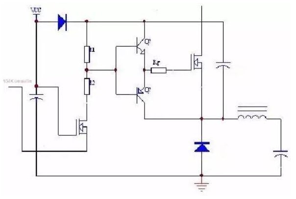
Fig.6
2: MOS driven directly by power IC
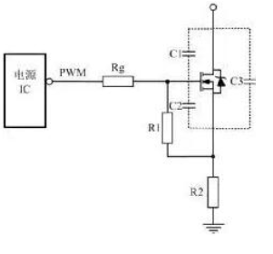
Fig.7
Power IC direct drive is the most commonly used drive mode, but also the simplest drive mode, using this drive mode, we should pay attention to a few parameters and the impact of these parameters. First, check the power IC manual, and its maximum drive peak current, because different chips and drive capacities are often not the same. Second, understand the parasitic capacitance of MOSFET, as shown in Figure 2, C1 and C2 values. If the values of C1 and C2 are relatively large, the energy required for MOS tube conduction is relatively large; if the power supply IC does not have a relatively large drive peak current, then the speed of tube conduction is relatively slow. If the driving capacity is insufficient, high frequency oscillation may occur on the rising edge. Even if Rg is reduced in Figure 2, this will not solve the problem! IC driving capacity, MOS parasitic capacitance, MOS transistor switching speed, and other factors all affect the selection of driving resistance value, so Rg cannot be infinitely reduced.
3: When the POWER supply IC driving capacity is insufficient
If the parasitic capacitance of the MOS tube is relatively large, and the driving capability of the POWER IC is insufficient, the driving capability should be enhanced on the drive circuit. A totem pole circuit is often used to increase the driving capability of the power IC.
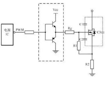
Fig.8
The purpose of this drive circuit is to increase the current supply capability and quickly complete the charging process of the input capacitive charge to the gate. This topology increases the time required for conducting, but reduces the turn-off time, allowing the switch tube to open quickly and avoiding high frequency oscillations along the rising edge.
4. The drive circuit accelerates MOS tube shutdown time
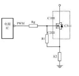
Fig.9
The turn-off instantaneous drive circuit can provide a path with as low impedance as possible for rapid discharge of capacitor voltage between MOSFET gate source poles, ensuring fast turn-off of the switch tube. To achieve rapid discharge of capacitive voltage between the gate source electrodes, a resistor, and a diode are usually connected in parallel on the drive resistance, as shown in Figure 4, where D1 is commonly used as the fast recovery diode. This reduces the turn-off time and the loss during the turn-off. Rg2 is to prevent too much current when the power is turned off and burn off the POWER IC.
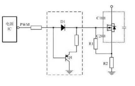
Fig.10
The totem pole circuit introduced in the second point also speeds up the turn-off. When the driving capacity of the power IC is sufficient, the circuit in Figure 2 can be improved to accelerate the MOS tube shutdown time, and the circuit shown in Figure 4 can be obtained. It is common to use a triode to drain the capacitance voltage between grid source electrodes. If the Q1 emitter has no resistance, when the PNP triode is switched on, the capacitance between the grid source electrodes will be shortened, to discharge the charge in the shortest time and minimize the cross loss during the shutdown. Compared with the topology in Figure 3, another advantage is that the current does not pass through the power IC when the charge is discharged from the capacitance between the gate source electrodes, which improves reliability.
5: The drive circuit accelerates the MOS tube turn-off time
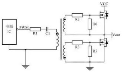
Fig.11
To satisfy the drive of a high-end MOS tube as shown in Figure 5, a transformer drive is often used, and sometimes transformer drive is also used to satisfy the safety isolation. The purpose of R1 is to inhibit the parasitic inductance on the PCB from forming LC oscillation with C1, which is to separate the DC and prevent the saturation of the magnetic core through AC.
In addition to the above drive circuit, there are many other forms of drive circuit. For a variety of driving circuits, not a driving circuit is the best, only combined with the specific application, choose the most appropriate driver.
- +1 Like
- Add to Favorites
Recommend
- Details of MOS tube packaging
- The Differences between MOS Tube and IGBT Tube
- Explain in Detail the Cause of MOS Tube Heating
- What is the Difference between MOS tube and IGBT?
- MOS Tube Knowledge, Must Read!
- How to Judge the Working State of MOS Tube?
- MOS Tube Anti-overvoltage Circuit
- Analysis of Classic MOS Tube Drive Circuit
This document is provided by Sekorm Platform for VIP exclusive service. The copyright is owned by Sekorm. Without authorization, any medias, websites or individual are not allowed to reprint. When authorizing the reprint, the link of www.sekorm.com must be indicated.
Integrated Circuits


Discrete Components


Connectors & Structural Components


Assembly UnitModules & Accessories


Power Supplies & Power Modules


Electronic Materials


Instrumentation & Test Kit


Electrical Tools & Materials


Mechatronics


Processing & Customization


