Analysis of Classic MOS Tube Drive Circuit


When making a power supply or drive, a power device MOS tube is the most commonly used device. When using an MOS tube, if some parameters of the MOS tube are not carefully considered, the circuit is usually unable to work.
MOS tubes are widely used in circuits we are familiar with, such as switching power supplies, electric motors, lighting dimming, and other driving circuits. In this application, we generally use low-voltage MOS tubes. The high-voltage MOS tube is corresponding to the low-voltage MOS tube. The classification of these two MOS tubes is based on voltage. Generally, the voltage of the high-voltage MOS tube is around 400V-1000V, which can provide effective lock protection operation. The use of CMOS technology, compared with the bipolar driver, has low power consumption, and high operating efficiency, and can also improve the reliability of the system. Low voltage MOS tube voltage around 1V-40V, high speed, high performance, low power consumption, low on-resistance, small package, and other advantages, suitable for protection circuit and switching circuit.
Today's MOS drivers have several special applications:
1. Low-voltage application: when a 5V power supply is used, if a traditional totem pole structure is used at this time, the voltage drop of the BE audion is about 0.7V, resulting in the actual voltage finally added to the gate being only 4.3V. At this time, there is a certain risk when we choose THE MOS tube with a nominal GATE voltage of 4.5V. The same problem occurs with 3V or other low-voltage sources.
2. Wide voltage applications: The input voltage is not a fixed value, it will change with time or other factors. This change causes the drive voltage supplied by THE PWM circuit to the MOS tube to be unstable.
To make MOS tubes safe under high gate voltage, many MOS have voltage regulators installed in the tubes to forcibly limit the amplitude of gate voltage. In this case, when the supplied driving voltage exceeds the voltage of the regulator tube, a large static power consumption will be caused.
At the same time, if we simply reduce the GATE voltage by using the principle of resistor divider, the MOS tube will work well when the input voltage is high, but when the input voltage is low, the GATE voltage is insufficient, causing insufficient conduction and thus increasing the power consumption.
3. Dual voltage applications: In some control circuits, the logic portion USES a typical digital voltage of 5V or 3.3V, while the power portion USES a voltage of 12V or more. The two voltages are connected in common ground mode. This requires the use of a circuit so that the low-voltage side can effectively control the HIGH-voltage side of the MOS tube. Meanwhile, the high-voltage side of the MOS tube will also face the problems mentioned in 1 and 2.
In these three cases, the totem pole structure can not meet the output requirements, and for many off-the-shelf MOS drive ICs, it seems that there is no structure containing a gate voltage limit. Two relatively common circuits are Shared to satisfy the above three application scenarios.
The circuit diagram is as follows:
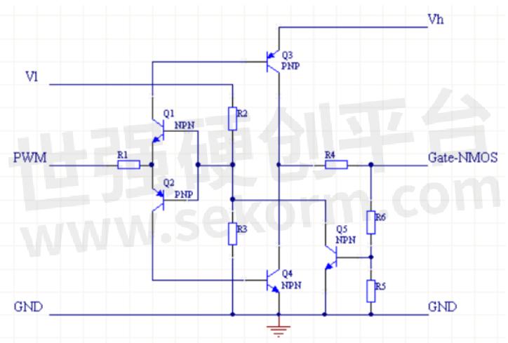
Fig.2Drive circuit for NMOS
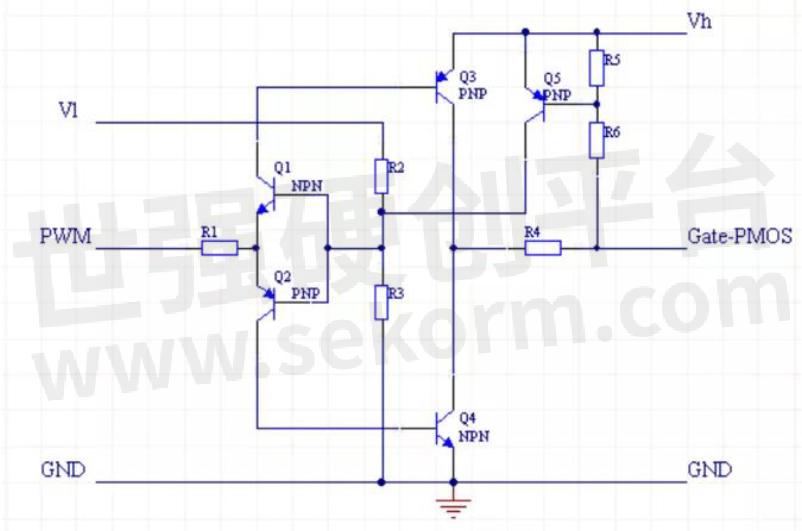
Fig.3 Driver circuit for PMOS
The NMOS and PMOS drive circuits in the figure above have the same function. Here, only the NMOS drive circuit is analyzed:
VL and VH are low-end and high-end power supplies respectively. The two voltages can be the same, but VL should not exceed VH.
Q1 and Q2 form an inverted totem pole to achieve isolation while ensuring that the two drive tubes Q3 and Q4 do not simultaneously conduct.
R2 and R3 provide PWM voltage reference, and by changing this reference, the circuit can be operated in the position where THE PWM signal waveform is relatively steep.
Q3 and Q4 are used to provide driving current. When conducting, both Q3 and Q4 have a minimum VCE drop relative to VH and GND, which is usually only about 0.3V, much lower than the 0.7V VCE.
R5 and R6 are feedback resistors, which are used to sample gate voltage. The sampled voltage generates strong negative feedback to the base of Q1 and Q2 through Q5, thus limiting gate voltage to a limited value. This value can be adjusted by R5 and R6.
Finally, R1 provides the base current limit of Q3 and Q4, and R4 provides the gate current limit of the MOS tube, namely the limit of Ice of Q3 and Q4. If necessary, the capacitors can be accelerated in parallel on R4.
This circuit provides the following features:
Drive high-end MOS tube with low voltage and PWM;
MOS tube with high GATE voltage requirement is driven by a small amplitude PWM signal;
Gate voltage peak limit;
Current limits for input and output;
By using the right resistance, very low power consumption can be achieved;
PWM signal reverse phase. NMOS does not require this feature and can be solved by prefacing an inverter.
Totem poles have been mentioned many times, but here's what totem poles are.
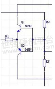
Fig.4
The totem pole is a transistor on the upper and lower sides, the upper tube is NPN, the c pole is connected to the positive power supply, the lower tube is PNP, the E pole is connected to the negative power supply, note, is the negative power supply, is the ground. Two B poles are connected for input, e of the upper pipe, and C of the lower pipe are connected for output. Used to match voltage, or improve IO port drive capability.
As the above circuit analysis, the use of an MOS tube involves a lot of knowledge points, I hope you can correctly standardize the use of an MOS tube, and give play to its maximum value.
- +1 Like
- Add to Favorites
This document is provided by Sekorm Platform for VIP exclusive service. The copyright is owned by Sekorm. Without authorization, any medias, websites or individual are not allowed to reprint. When authorizing the reprint, the link of www.sekorm.com must be indicated.
Recommend

Switching Power Supply MOS Tube Loss
2024-02-19 - Design Article Switch Mode Power Supply, also known as switched Power Supply, switching converter, is a high-frequency Power conversion device, is a kind of Power Supply. Its function is to convert a potential voltage through different forms of architecture to the voltage or current required by the client. Switching power supplies convert voltages and currents between the inputs, which are mostly AC (such as mains power) or DC power, and the outputs, which are mostly devices requiring DC power, such as personal computers.
MOS Tube Drive Circuit Summary - Detailed Design of Various Switching Power Supply MOS Tube Drive Circuit
2024-02-24 - Design Article When using MOS tube drive circuit to design switch power supply or motor drive circuit, most people will consider MOS conduction resistance, maximum voltage, maximum current, etc., and many people only consider these factors. Such circuits may work, but they are not excellent and are not allowed as a formal product design.
Explain in Detail the Cause of MOS Tube Heating
2024-02-27 - Design Article For power supply design or driving circuit, it is inevitable to use field effect tube, which is often called MOS tube. There are many kinds of MOS tubes and they have many functions. To do the use of power or drive, of course, is to use its switching action.Regardless of N type or P type MOS tube, the operating principle is essentially the same. MOS transistors control the drain current at the output end by applying voltage to the gate at the input end. MOS tube is a voltage control device.
Detailed explanation of MOS tube working principle diagram
2025-09-17 - Technical Discussion MOS transistor is one kind of FET (the other is JFET), which can be manufactured into enhanced or depleted type. There are four types of p-channel or n-channel, but only enhanced n-channel MOS transistor and enhanced p-channel MOS transistor are actually applied. Therefore, NMOS or PMOS are usually referred to.
The Differences between MOS Tube and IGBT Tube
2023-07-27 - Technical Discussion MOS tube is MOSFET, the Full Chinese name is metal-oxide-semiconductor field effect transistor, because the gate of this kind of field effect tube is isolated by the insulating layer, so it is also called insulated gate field effect tube.
How to design MOS tube drive circuits for different powers?
2025-06-11 - Technical Discussion In the process of power supply debugging, the debugging of driving signal is very important, which directly affects the reliability, efficiency, design temperature rise and EMC characteristics of the power supply. Therefore, the design of driving circuit is an important indicator of power supply design, and the rationality of driving parameters has a direct impact on all aspects of power supply performance.
MOS Tube Anti-overvoltage Circuit
2024-03-01 - Design Article When the power is properly connected. The current flows from VIN to the load, through NMOS to GND. At the beginning of power on, because the body diode of the NMOS tube exists, the ground circuit is connected through the body diode. Later, because the VGS is greater than the threshold voltage of VGSTH, the MOS tube conducts.
Details of MOS tube packaging
2024-02-10 - Technical Discussion After the MOS tube chip is made, a shell is needed to be added to the MOS tube chip, which is the MOS tube package. The package housing mainly plays the role of support, protection and cooling, and also provides electrical connection and isolation for the chip, so as to form a complete circuit between MOS tube devices and other components. Different packaging, different design, MOS tube specifications, size, various electrical parameters, etc. will be different, and they can play a different role in the circuit will be different.
Why Can AO8822 Dual Nmos Tube Be Widely Used in Home Appliances, Leds and Other Products?
2025-02-20 - Technical Discussion AO8822 products mainly play the role of switching and current and voltage regulation in the circuit. For example, in the motor driving circuit, the characteristics of AO8822 are suitable for various motor driving scenarios, including switching power supply products. Its extremely low on-resistance and high reliability help switching power supply products reduce energy loss and improve overall system efficiency.
The Drive Circuit Design of MOS Tube
2024-02-18 - Design Article In the power supply debugging process, the debugging of the drive signal is particularly important, which is not only for the reliability of the power supply, the efficiency of the power supply, the design temperature rise of the power supply, and EMC characteristics are particularly important. Therefore, the design of the drive circuit becomes an important index of the design power supply. The rationality of driving parameters directly affects the performance of the power supply.
How to Judge the Working State of MOS Tube?
2023-08-01 - Technical Discussion There are two working states of MOS tubes: enhanced and exhausted, divided into N channel and P channel. The MOS tube is the metal, oxide, and semiconductor field effect transistor, or the metal-insulator and semiconductor. This article we share how to judge the working state of a MOS tube.
MOS Tube HKTD20N06 with Continuous Drain Current of 20A, Can be Used in Motor Drive, LED and Power Supply Products
2024-11-20 - Product Introduction MOS transistor plays a very important role in voltage stabilizing and switching circuits. A good MOS transistor has not only good product performance, but also its power consumption and product stability. In this issue, Heketai introduces a MOS tube HKTD20N06, which can be used in motor drives, LEDs and power supplies.
Six Kinds of Universal MOS Tube Circuit Analysis
2024-02-12 - Design Article For MOS tube, many people are impressed by the small signal analysis model learned in the textbook of mode electricity, as well as various kinds of amplifying circuit. In practical projects, MOS transistors are often used in full-bridge drives, full-bridge inverters, Buck/Boost circuits and other circuits.
MOS Tube Knowledge, Must Read!
2024-02-26 - Technical Discussion According to the size of PCB board, select the appropriate PMOS tube size, in the case of limited on-board area, choose the small package as far as possible; As far as possible to select common packaging, to prepare for the subsequent selection of appropriate replacement material.
Application of MOS and Rectifier in Blower Products
2024-11-05 - Technical Discussion As a high-frequency electric product, hair dryer usually consists of heating wire, high-speed small fan and circuit board. There are usually metal blowers and plastic blowers, and the centrifugal airflow formed by the rotation of the blades driven by the motor drives the rotor to blow out to achieve the purpose of drying and shaping. In this issue, Heketai introduces the application of MOS and rectifier in hair dryer products.

Electronic Mall


 Auth. Dist.
Auth. Dist.
Auth. Dist.
Auth. Dist.
Auth. Dist.
Auth. Dist.
Auth. Dist.
Auth. Dist.
Auth. Dist.
Auth. Dist.
Auth. Dist.
Integrated Circuits


Discrete Components


Connectors & Structural Components


Assembly UnitModules & Accessories


Power Supplies & Power Modules


Electronic Materials


Instrumentation & Test Kit


Electrical Tools & Materials


Mechatronics


Processing & Customization


