Details of MOS tube packaging

After the MOS tube chip is made, a shell is needed to be added to the MOS tube chip, which is the MOS tube package. The package housing mainly plays the role of support, protection and cooling, and also provides electrical connection and isolation for the chip, so as to form a complete circuit between MOS tube devices and other components. Different packaging, different design, MOS tube specifications, size, various electrical parameters, etc. will be different, and they can play a different role in the circuit will be different; In addition, packaging is also an important reference for MOS tube selection in circuit design. The importance of encapsulation is self-evident.
MOS tube packaging classification
MOS tube packages can be divided into two main categories according to the way they are installed on THE PCB: Through Hole and Surface Mount.
The insertion type is the MOSFET pin that passes through the mounting hole of the PCB and is welded to the PCB. The plug-in package has a transistor profile package (TO).
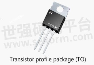
Fig.1 Plug in package
Surface mount is MOSFET pin and heat dissipation flange welding on the PCB surface of the solder pad. Typical surface-mounted packages include: D-PAK, SOT, SOP, etc. With the development of technology, fewer and fewer PCB boards, such as motherboards and video CARDS, adopt the straight-insert packaging mode, and more and more surface mount packaging mode is adopted.
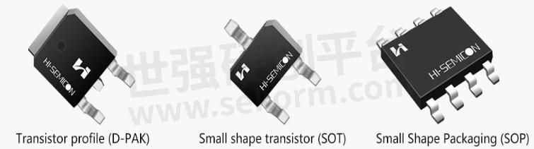
Fig.2 Surface mount packaging
1. Dual inline package (DIP)
The DIP package has two rows of pins, which need to be inserted into the chip socket with the DIP structure, and is derived from SDIP(Shrink), that is, the double-wire package is six times more dense than the DIP pin density.
DIP packaging structure forms include: multilayer ceramic double-row DIP, single-layer ceramic double-row DIP, lead frame DIP(including glass ceramic sealing type, plastic sealing structure type, ceramic low-melt glass packaging type). The DIP package features easy perforation welding of the PCB and good compatibility with the motherboard. But because its package area and thickness are relatively large, and pin is easy to be damaged in the process of plugging, the reliability is poor; At the same time, due to the influence of the process, there are generally no more than 100 pins, so in the highly integrated process of the electronics industry, DIP packaging gradually withdrew from the historical stage.
2. Transistor shape Packaging (TO)
It belongs TO the early packaging specifications, such as TO-3P, TO-247, TO-220, TO-220F, TO-251, to-263, etc., are all plug-in packaging designs.
TO-3P /247: It is the commonly used packaging form of medium and high voltage, large current MOS tube. The product has the characteristics of high voltage resistance, strong resistance TO wear, etc.
TO-220 /220F: TO-220F is fully plastic package. There is no need TO add insulation pad when it is installed on the radiator. The TO-220 has a metal strip attached TO the middle foot and an insulating pad for the radiator. The two encapsulated MOS tubes are similar in appearance and can be used interchangeably.
TO-251: The packaged product is designed TO reduce cost and reduce volume, and is mainly used in medium voltage environment with large current below 60A and high voltage below 7N.
In recent years, due TO the high welding cost of plug-in packaging process and the lower heat dissipation performance than SMT products, the market demand for SURface-mount packaging has been increasing, which also leads TO the development of TO packaging TO SURface-mount packaging. To-252 (also known as D-PAK) and to-263 (D2PAK) are surface mount packages.
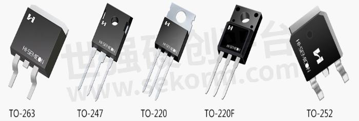
Fig.3 TO encapsulate the appearance of a product
TO-252 is a kind of plastic chip packaging, often used in the power transistor, voltage regulator chip packaging, is one of the mainstream packaging.
The MOSFET with the encapsulated mode has three electrodes, gate (G), drain (D) and source (S).
The pin of drain pole (D) is not cut, but the heat dissipation plate on the back is used as drain pole (D), which is directly welded to the PCB. On the one hand, it is used to output large current, and on the other hand, it can dissipate heat through THE PCB. Therefore, there are three d-PAK pads in PCB, and the drain pole (D) pad is larger. Its packaging specifications are as follows:
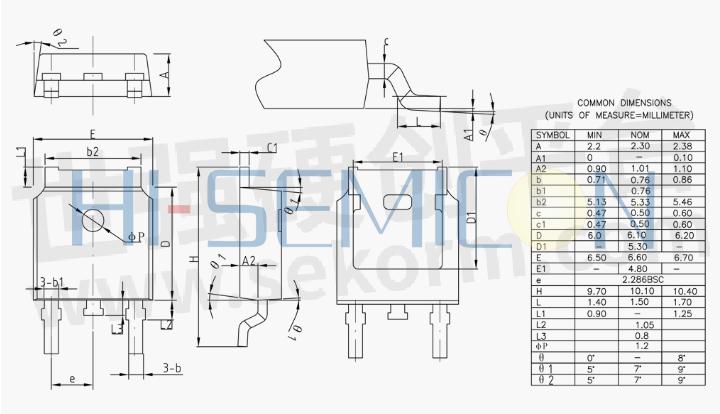
Fig.4 TO-252 Package size specification drawing
TO-263, a variant of TO-220, is designed TO improve production efficiency and heat dissipation, and supports extremely high current and voltage. It is more common in MEDIUM-voltage and high-current MOS tubes of less than 150A and more than 30V.In addition TO D2PAK(TO-263AB), also includes TO263-2, TO-263-3, TO-263-5, TO-263-7 and other styles, and TO-263 for the dependency relationship, mainly lead TO the number of feet and distance is different.
Fig.5 TO-263 Package size specification drawing
Small shape transistor Package (SOT)
The SOT(Small-Out-of-line transistorized) is a Small power transistorized sugar-patch type consisting of SOT-23-6L and SOT-23-3L, whose volume is smaller than that of TO.
Fig.6SOT encapsulates the type diagram
SOT-23 is a common triode packaging forms, there are three wing shape pins, the collector and emitter and the base, respectively, in components on both sides of long sides respectively, among them, the emitter and the base on the same side, common in small power transistors, field effect tube and the compound transistor with resistance network, good strength, but poor weldability, shape of (a) as shown in the diagram below.
Small Shape Packaging (SOP)
SOP(Small-out-of-line Package) is one of the surface-mounted packages, also known as SOL or DFP. The pins are drawn from both sides of the Package in the shape of a seagull wing (L-shaped). There are plastic and ceramic materials.
SOP packaging standards include SOP-8, SOP-16, SOP-20, SOP-28, etc. The number after SOP represents the number of pins. MOSFET's SOP packaging mostly USES the SOP-8 specification, and the industry often omits the "P" and abbreviates it as SO(small-out-of-line).
SOP-8 package dimensions
SOP-8 is the first developed by PHILIP company. It adopts plastic package, no heat dissipation baseplate, poor heat dissipation, generally used for low power MOSFET.
After that, TSOP(thin and small shape packaging), VSOP(very small shape packaging), SSOP(reduced type SOP), TSSOP(thin and reduced type SOP) and other standard specifications are gradually derived. TSOP and TSSOP are commonly used in MOSFET encapsulation.
- +1 Like
- Add to Favorites
Recommend
- The Differences between MOS Tube and IGBT Tube
- MOS Tube Drive Circuit Summary - Detailed Design of Various Switching Power Supply MOS Tube Drive Circuit
- Explain in Detail the Cause of MOS Tube Heating
- What is the Difference between MOS tube and IGBT?
- MOS Tube Knowledge, Must Read!
- How to Judge the Working State of MOS Tube?
- MOS Tube Anti-overvoltage Circuit
- Analysis of Classic MOS Tube Drive Circuit
This document is provided by Sekorm Platform for VIP exclusive service. The copyright is owned by Sekorm. Without authorization, any medias, websites or individual are not allowed to reprint. When authorizing the reprint, the link of www.sekorm.com must be indicated.
Integrated Circuits


Discrete Components


Connectors & Structural Components


Assembly UnitModules & Accessories


Power Supplies & Power Modules


Electronic Materials


Instrumentation & Test Kit


Electrical Tools & Materials


Mechatronics


Processing & Customization


