How to Judge the Working State of MOS Tube?

How to judge the working state of the MOS tube
There are two working states of MOS tubes: enhanced and exhausted, divided into N channel and P channel.
The MOS tube is the metal, oxide, and semiconductor field effect transistor, or the metal-insulator and semiconductor. The source of the MOS tube and the drain can be switched, and they are both n-type areas formed in the P-TYPE Backgate. In most cases, the two regions are the same, and the switching of the two ends does not affect the performance of the device. Such devices are considered to be symmetrical.
How to judge the working status of MOS tube -N channel enhanced MOS field effect tube
1. Control the effect of VGS on ID and channel
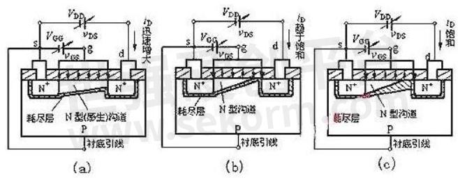
①. VGS=0
It can be seen from FIG. 1(a) that there are two PN junctions back-to-back between drain D and source S of the enhanced MOS tube. When the grid-source voltage VGS=0, even if the drain-source voltage VDS is added, and no matter what the polarity of VDS is, there is always a PN junction in the reversed state, and there is no conductive channel between the drain-source poles, so the drain current ID≈0 in this case.
②. VGS>0 situation
In the case of VGS > 0, an electric field is generated in the SiO2 insulation layer between the gate and substrate. An electric field is directed from the gate to the substrate perpendicular to the semiconductor surface. This electric field repels holes and attracts electrons.
Repulsive hole: The hole in the P-type substrate near the gate is repelled, leaving the immovable acceptor ion (negative ion), forming the depletion layer. Electron attraction: The attraction of electrons (electrons) from a P-TYPE substrate to the surface of the substrate.
2. Formation of conductive channel:
When the VGS value is small and the ability to attract electrons is not strong, there is still no conductive channel between leakage and source electrodes, as shown in FIG. 1(b). VGS increases, the increase in the number of electrons attracted to the substrate surface P, when the VGS reaches a certain value, the electrons in the grid near the substrate surface form a P N thin layer, and with two connected to the N + area, formed in the leak - source electrode N-type conductive channel, the conductive type, in contrast to the P substrate, so it is also called the inversion layer, as shown in figure 1 (c). The larger the VGS, the stronger the electric field on the semiconductor surface, the more electrons are attracted to the P substrate surface, the thicker the conductive channel, and the smaller the channel resistance.
The gate-source voltage at the beginning of the channel formation is called the open voltage and is denoted by VT.
The N-channel MOS tube discussed above cannot form a conductive channel when VGS < VT and the tube is in a cut-off state. Channel formation occurs only when VGS≥VT. This kind of MOS tube which must be at VGS≥VT to form a conductive channel is called an enhanced MOS tube. After the channel is formed, a drain current is generated by adding a positive voltage VDS between the drain and source electrodes.
The impact of VDS on ID
(1) Structure: The N-channel depletion MOS tube is basically similar to the N-channel enhancement MOS tube.
(2) Difference: When VGS=0 for the depletion MOS tube, a conductive channel exists between the leakage-source electrode, while the conductive channel appears only when VGS≥VT for the enhanced MOS tube.
(3) reasons: manufacturing n-channel depletion, MOS tubes are mixed with a large amount of alkali metal cations in SiO2 insulation Na + and K + (manufacturing P channel depletion MOS tube with negative ions), as shown in figure 1 (a), so even if VGS = 0, the effects of the electric field in the positive ion, leak - source electrode p-type substrate surface can also generate N channel induction (referred to as the initial channel), as long as plus forward voltage, VDS have current ids.
If positive VGS are added, the electric field between the gate and N channel will attract more electrons in the channel, the channel will be widened, the channel resistance will become smaller, and the ID will increase. On the contrary, when VGS is negative, the induced electrons in the channel decrease, the channel Narrows, the channel resistance increases, and the ID decreases. When VGS increases negatively to a certain value, the conductive channel disappears, ID tends to zero, and the pipe is cut off, so it is called the depletion type. The grid-source voltage when the channel disappears is called the clipping voltage, which is still expressed by VP. Similar to the N-channel junction fET, the clipping voltage VP of the N-channel depletion MOS tube is also negative, but the former can only work under the condition of VGS<0. And this is VGS=0, VGS>0.
Curve and current equation of N channel enhanced MOS tube
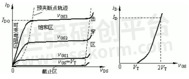
Output characteristic curve
The output characteristic curve of the n-channel enhanced MOS tube is shown in Figure 1(a). Like junction ET, its output characteristic curve can be divided into variable resistance area, saturation area, cut-off area, and breakdown area. Transfer characteristic curve as shown in figure 1 (b), when used for amplification of the field effect tube device is working in a saturated zone (constant current), the ID hardly changes with VDS, namely different VDS of the transfer characteristic curve is almost overlap, so the available VDS is greater than a certain value (> VGS VDS - VT) after a transfer characteristic curve instead of the saturated zone all transfer characteristic curve.? The approximate relationship between ID and VGS.Similar to junction ET. In the saturation region, the approximate relationship between ID and VGS is:
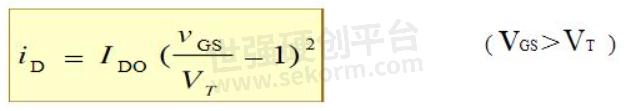
In the equation, IDO is the drain current ID when VGS=2VT
P channel depletion MOS tube
P channel MOSFET works exactly the same as N channel MOSFET, except that the conductive carriers are different and the supply voltage polarity is different. This is similar to the bipolar transistor having NPN and PNP transistors.
- +1 Like
- Add to Favorites
Recommend
- Details of MOS tube packaging
- The Differences between MOS Tube and IGBT Tube
- MOS Tube Drive Circuit Summary - Detailed Design of Various Switching Power Supply MOS Tube Drive Circuit
- Explain in Detail the Cause of MOS Tube Heating
- What is the Difference between MOS tube and IGBT?
- MOS Tube Knowledge, Must Read!
- MOS Tube Anti-overvoltage Circuit
- Analysis of Classic MOS Tube Drive Circuit
This document is provided by Sekorm Platform for VIP exclusive service. The copyright is owned by Sekorm. Without authorization, any medias, websites or individual are not allowed to reprint. When authorizing the reprint, the link of www.sekorm.com must be indicated.
Integrated Circuits


Discrete Components


Connectors & Structural Components


Assembly UnitModules & Accessories


Power Supplies & Power Modules


Electronic Materials


Instrumentation & Test Kit


Electrical Tools & Materials


Mechatronics


Processing & Customization


