MOS Switch Tube Selection and Principle Application

Generally, for MOS with a high-end drive, the gate voltage is larger than the source voltage for on-off conduction, while for MOS with a high-end drive, the source voltage is the same as the drain voltage (VCC), so the gate voltage is 4V or 10V larger than the VCC. If you want to get a higher voltage than the VCC in the same system, you need a dedicated boost circuit. Many motor drivers are integrated with charge pumps. It should be noted that appropriate external capacitors should be selected to obtain sufficient short-circuit current to drive the MOS tube.
MOS tube is voltage-driven, it should be said that as long as the grid voltage to the open voltage can conduct DS, the grid series can conduct any resistance. But if required at the high switching frequency, the gate to ground or VCC can be seen as a capacitor, for a capacitor, the greater the resistance of string, grid to conduction voltage, the longer the MOS is conducting state, the longer time and in a conducting state resistance is bigger, fever also increases, easy to damage the MOS, so high frequency grid series resistance not only smaller, usually to add front drive circuit.
Basic knowledge of MOS tube switch
1. MOS type and structure
MOSFET tube is one kind of FET (the other is JFET), which can be manufactured into enhanced or exhausted types. There are four types of P channel or N channel but only enhanced N channel MOS tube and enhanced P channel MOS tube are used in practice. Therefore, NMOS is usually mentioned, or PMOS refers to these two types. For these two kinds of enhanced MOS tubes, NMOS is the most commonly used one -- because the on-off resistance is small and easy to manufacture, so NMOS is generally used in the applications of switching power supplies and motor drives.
There is parasitic capacitance between the three pins of the MOS tube, which is not what we need but is caused by manufacturing process limitations. The existence of parasitic capacitance makes it difficult to design or select a drive circuit, but there is no way to avoid it, which will be described in detail later. Between the drain and source of the MOS tube is a parasitic diode called a bulk diode, which is important in driving inductive loads such as motors. By the way, volume diodes exist only in a single MOS tube, not usually in an IC chip.
2. Conduction characteristics of MOS tube
To conduct means to act as a switch, equivalent to a switch being closed.
NMOS features that when the VGS is greater than a certain value, it will conduct. It is suitable for the situation when the source is grounded (low-end drive), as long as the gate voltage reaches 4V or 10V. PMOS features, VGS less than a certain value will be conductive, suitable for source pole VCC (high-end driver). However, although PMOS can be easily used as high-end drivers, NMOS is usually still used in high-end drivers due to its high on-off resistance, high price, and few replacement types.
3. MOS switch tube loss
Whether it is NMOS or PMOS, there is a conduction resistor after the conduction, so the current will consume energy on this resistor. This part of the energy consumed is called the conduction loss. Choosing an MOS tube with small conduction resistance will reduce conduction loss.
The current small power MOS tube conduction resistance is generally in the tens of milliohms, a few milliohms are also available. MOS must not be done instantaneously when conducting and cutting off. The voltage at both ends of MOS has a descending process, while the current flowing through it has a rising process. During this period, the loss of the MOS tube is the product of voltage and current, which is called switch loss. Generally, the switch loss is much greater than the on-off loss, and the faster the switch frequency, the greater the loss.
The product of transient voltage and current is very large, and the loss is also very large.
Shortening the switching time can reduce the loss of each conduction. Reducing the switching frequency can reduce the number of switches per unit of time. Both methods can reduce switch loss.
4. MOS tube drive
Compared with bipolar transistors, it is generally believed that MOS tube conduction does not require current, as long as the GS voltage is higher than a certain value, it is ok. That's easy to do, but we also need speed.
In the structure of the MOS tube, it can be seen that there is parasitic capacitance between GS and GD, while the drive of the MOS tube is the charge and discharge of the capacitor. A current is needed to charge the capacitor because the capacitor can be regarded as a short circuit at the moment of charging, so the instantaneous current will be relatively large. The first thing to note when selecting/designing MOS tube drives is the size of the instantaneous short-circuit current that can be provided.
In the selection of MOSFET, there are two types of MOSFET: N channel and P channel. In power system, MOSFET can be regarded as an electrical switch. When a positive voltage is applied between the gate and the source of the N-channel MOSFET, the switch conductance is on. During conduction, the current can flow from the drain to the source via a switch. There is an internal resistance between the drain and the source, called ON resistance RDS(ON).
It is important to know that the MOSFET gate is a high-impedance end, so always add a voltage to the gate, which is the resistance to the ground that the gate is connected to in the circuit diagram below. If the gate is suspended, the device will not work as intended and may turn on or off at inappropriate times, resulting in potential power losses to the system. When the voltage between the source and the gate is zero, the switch closes and the current stops passing through the device. Although the device has been turned off, there is still a small current, which is called leakage current, or IDSS.
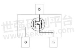
Fig.1
N channel or P channel?
The first step in choosing the right device for design is to decide whether to use n-channel or P-channel MOSFET. In typical power applications, when a MOSFET is grounded and the load is connected to the mainline voltage, the MOSFET constitutes a low-voltage side switch. N channel MOSFET should be used in the low voltage side switch for consideration of the voltage required to close or conduct the device.
High voltage side switches are used when the MOSFET is connected to the bus and load ground. The P-channel MOSFET is usually used in this topology, again due to voltage drive considerations.
Determine rated current
The second step is to select the MOSFET-rated current, which, depending on the circuit structure, should be the maximum current that the load can withstand under all circumstances. Similar to the voltage case, the designer must ensure that the SELECTED MOSFET can withstand the rated current, even when the system is generating peak current. The two current cases considered are the continuous mode and the pulse spike.
In the continuous mode, the MOSFET is in a steady state, and the current flows continuously through the device. A spike is a device that has a large surge (or spike current) flowing through it. Once the maximum current under these conditions is determined, you can simply select the device that can withstand the maximum current.
After the rated current is selected, the conduction loss must also be calculated. In practice, MOSFET is not an ideal device because of the power loss during conduction, which is called the conduction loss. The MOSFET ACTS as a variable resistor when "ON", determined by the DEVICE's RDS(ON), and varies significantly with temperature.
The power loss of the device can be calculated by Iload2×RDS(ON). Since the on-resistance changes with temperature, the power loss will also change proportionally. The higher the voltage VGS applied to the MOSFET, the smaller the RDS(ON) will be, and conversely, the higher the RDS(ON) will be. For the system designer, this is where the tradeoff depends on the system voltage. Lower voltages are easier (and more common) for portable designs and higher voltages for industrial designs. Note that the RDS(ON) resistance increases slightly with the current. Variations in the electrical parameters of the RDS(ON) resistance can be found in the technical data sheet provided by the manufacturer.
Determine thermal requirements
The next step in selecting MOSFET is to calculate the cooling requirements of the system. The designer must consider two different scenarios, the worst case and the true case. A worst-case calculation is recommended because it provides a greater margin of safety to ensure that the system does not fail. There are also some important measurements on the MOSFET datasheet, such as the thermal resistance between the semiconductor junction and the environment of the packaged device, and the maximum junction temperature.
The junction temperature of the device is equal to the maximum ambient temperature plus the product of thermal resistance and power dissipation (junction temperature = maximum ambient temperature +[thermal resistance × power dissipation]). According to this equation, the maximum power dissipation of the system can be solved, that is, it is equal to I2×RDS(ON) by definition. Since the designer has determined the maximum current to pass through the device, RDS(ON) at different temperatures can be calculated. It is important to note that when working with simple thermal models, the designer must also consider the thermal capacity of the junction/device housing and the housing/environment, which requires that the PRINTED circuit boards and packages do not heat up immediately.
Usually, in a PMOS transistor pipe, there will be a parasitic diode, the diode is used to prevent the reverse leakage source end, for the PMOS transistor, the NMOS advantage is that it can open voltage is 0, the DS voltage between the voltage difference is not big, and NMOS conduction conditions required VGS is greater than the threshold, this will lead to the control voltage is greater than the required voltage, will appear the unnecessary trouble.
PMOS is selected as the control switch, and there are two applications as follows:
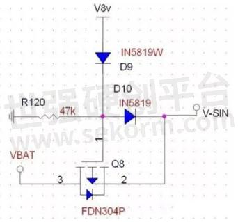
Fig.2
PMOS is used to select the voltage. When V8V exists, the voltage is all provided by V8V, and the PMOS is turned off. VBAT does not provide the voltage to VSIN, but when V8V is low, VSIN is supplied by 8V. Note the grounding of R120, which can steadily lower the grid voltage and ensure the normal opening of PMOS, which is also a potential state hazard caused by the high grid impedance described above. The function of D9 and D10 is to prevent voltage backfilling. D9 can be omitted. It should be noted here that the DS connection of the circuit is reversed so that the function of the switch tube cannot be achieved due to the epidiode conduction, so pay attention to the practical application.
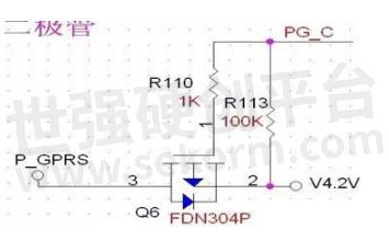
Fig.3
Looking at this circuit, the control signal PGC controls whether V4.2 supplies power to P_GPRS. In this circuit, the two ends of the source leakage are not connected backward. The significance of the existence of R110 and R113 is that the current of the R110 control gate is not too large, and the normal state of the R113 control gate is to pull up R113 to a high level up to PMOS, which can also be regarded as the pull up of the control signal. When the internal pin of the MCU is not pulled up, that is, when the output is an open leak, the PMOS cannot be driven off. In this case, the pull-up given by the external voltage is needed, so the resistor R113 plays two roles. The R110 can be smaller, up to 100 ohms.
Switching characteristics of MOS tube
Static characteristic
As a switching element, the MOS tube also works in two states of cut-off or conduction. As THE MOS tube is a voltage control element, its operating state is mainly determined by the gate-source voltage UGS.
Working characteristics are as follows:
The UGS opening voltage UT: MOS transistor works in the cut-off region, the drain-source current IDS is 0, the output voltage UDS≈UDD, and the MOS transistor is in the "off" state. Its equivalent circuit is shown in the figure below.
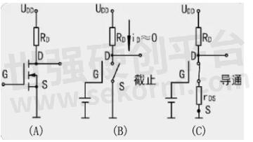
Fig.4
UGS > UT: MOS tube operating in the conduction zone, leakage source current IDS=UDD/(RD+RDS). Where RDS is the leakage source resistance of the MOS tube during conduction. Output voltage UDS=UDD·RDS/(RD+ RDS), if RDS "RD", UDS ≈0V, MOS tube is in the state of "on", its equivalent circuit is shown in the figure above (c).
The dynamic characteristics
The MOS tube also has a transition process when the conduction and cut-off states are transferred, but its dynamic characteristics mainly depend on the time required for charging and discharging of stray capacitance related to the circuit, while the time for charge accumulation and dissipation at the conduction and cut-off of the tube itself is very small. The following figure respectively shows the circuit composed of an NMOS tube and its dynamic characteristics.
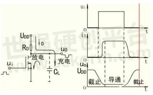
Fig.5 NMOS tube dynamic characteristics diagram
When the input voltage UI changes from high to low and the MOS tube changes from the on-off state to the cut-off state, the power UDD charges the stray capacitance CL via RD, charging time constant 1=RDCL, so the output voltage UO must pass a certain delay to change from the low level to the high level.
When the input voltage UIS changed from low to high and the MOS tube changed from the cut-off state to the on-off state, the charge on the stray capacitance CL passes RDS for discharge, and the discharge time is constant at 2≈RDSCL. As you can see, the output voltage Uo also has to undergo a certain delay before it can be converted to a low level. But because RDS is much smaller than RD, the transition time from cut off to lead is shorter than the transition time from lead to cut off.
Since the drain-source resistor, RDS is much larger than the saturation resistor RCES of the transistor, and the drain-external resistor RD is also larger than the transistor collector resistor RC, the charging and discharging time of the MOS tube is longer, so the switching speed of the MOS tube is lower than that of the transistor. However, in THE CMOS circuit, because the charging circuit and discharging circuit are low resistance circuits, the charging and discharging process is relatively fast, so the CMOS circuit has a higher switching speed.
- +1 Like
- Add to Favorites
Recommend
- MOS Tube Drive Circuit Summary - Detailed Design of Various Switching Power Supply MOS Tube Drive Circuit
- The Differences between MOS Tube and IGBT Tube
- What is the Difference between MOS tube and IGBT?
- Miller Effect on MOS Tube Switches
- Explain in Detail the Cause of MOS Tube Heating
- Analysis of Classic MOS Tube Drive Circuit
- MOS Tube Knowledge, Must Read!
- Switching Power Supply MOS Tube Loss
This document is provided by Sekorm Platform for VIP exclusive service. The copyright is owned by Sekorm. Without authorization, any medias, websites or individual are not allowed to reprint. When authorizing the reprint, the link of www.sekorm.com must be indicated.
Integrated Circuits


Discrete Components


Connectors & Structural Components


Assembly UnitModules & Accessories


Power Supplies & Power Modules


Electronic Materials


Instrumentation & Test Kit


Electrical Tools & Materials


Mechatronics


Processing & Customization


