Miller Effect on MOS Tube Switches

The basic principle of formation of Miller platform
The gate drive process of MOSFET can be simply understood as the charging and discharging process of the input capacitance (mainly CGS of the gate source capacitance) of the MOSFET. When THE CGS reaches the threshold voltage, MOSFET will enter the opening state. When MOSFET is opened, VDS starts to decline and ID starts to rise. At this time, MOSFET enters the saturated region. However, due to Miller effect, VGS will not rise for a period of time. At this time, ID has reached the maximum, while VDS continues to decline until Miller capacitor is fully charged and VGS rises to the value of the driving voltage. At this time, MOSFET enters the resistance area, VDS completely drops and the opening ends.
Because miller capacitors prevent VGS from rising, they prevent Vds from falling, thus increasing the time to wear out. (When VGS goes up, the conduction resistance goes down, thus VDS goes down)
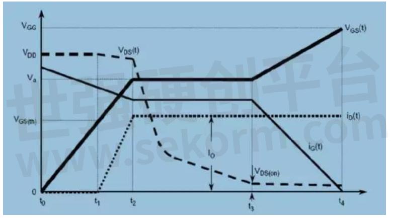
Fig.1
Miller effect is notorious in MOS drive. It is caused by the miller capacitance of the MOS tube. During the opening process of the MOS tube, the GS voltage rises to a certain voltage value and then becomes stable for some time, after which the GS voltage starts to rise again until complete conduction. Why is there a stable value here? Before the MOS is switched on, the D-pole voltage is greater than the G-pole voltage, and the electric quantity stored by the MOS parasitic capacitor CGD needs to be neutralized by the G pole injected during its conduction because the G-pole voltage is greater than the D-pole voltage after the MOS is fully switched on. The Miller effect will greatly increase the opening loss of MOS. (The MOS tube cannot be switched on very quickly)
So there comes the so-called totem drive!! When MOS is selected, the smaller the CGD is, the smaller the switching loss will be. The Miller effect is unlikely to disappear entirely.
Miller platform in MOSFET is a typical symbol of MOSFET being in the "big zone".
Using an oscilloscope to measure the GS voltage, you can see that there is a platform or pit during the voltage rise, this is the Miller platform.
The detailed process of formation of the Miller platform
The Miller effect refers to the miller platform produced in the opening process of the MOS tube switches. The principle is as follows.
In theory, the Miller effect can be eliminated by adding enough capacitance between the G and S stages of the drive circuit. But the switching time will drag on for a long time. The general recommendation plus a capacitance value of 0.1CIESS is beneficial.
The gentle part in the thick black line below is the Miller platform.
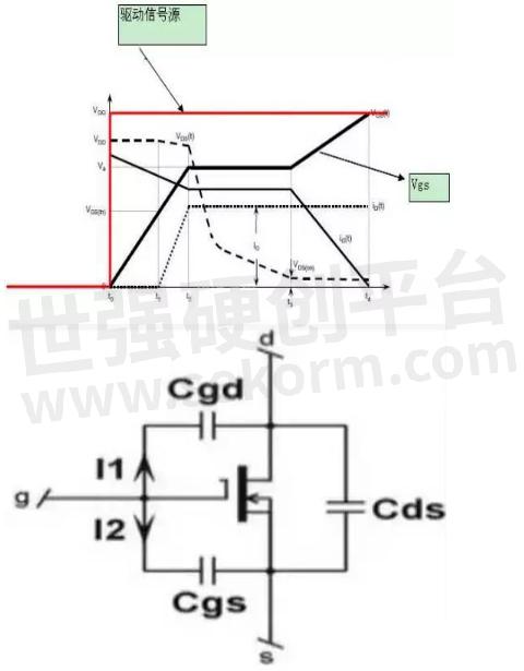
Fig.2
This diagram shows the delay-charge coefficient at the first turning point: VDS starts conduction. The variation of VDS forms a differential through CGD and the internal resistance of the driver source. Since VDS is approximately linearly decreasing, linear differentiation is a constant, resulting in a platform at VGS.
Miller platform is caused by the capacitance at both ends of MOS GD, namely CRSS in the MOS datasheet.
This process is to charge THE CGD, so the VGS changes very little. When the CGD is charged to the VGS level, the VGS will continue to rise.
When MOS was just opened, CGD discharged rapidly through MOS, and then the drive voltage was reversed charged, which Shared the drive current, making the voltage rise on CGS slow and the platform appeared.
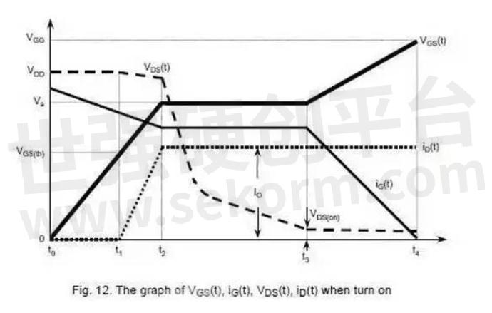
Fig.3
T0 ~ T1: VGS from 0 to VTH Mosfet not through Current by parasitic diode DF
T1 ~ T2: VGS from VTH to Va ID
T2 ~ T3: VDS decreases, The higher the current continues to pass through CGD VDD, the longer the time required.
IG is the driving current
It starts to get healthier faster When VDG approaches zero, CGD increases Until VDG becomes negative, CGD increases to the maximum IG decreases slowly
T3 ~ T4: complete conduction of Mosfet, operating in resistance zone VGS continues to rise to VGG

Fig.4
In the later stage of the platform, VGS continued to grow, and IDS changed little because MOS was saturated. However, from the picture of the building owner, this platform still had a length
During this platform, it can be considered that MOS is in the amplification period
Before the previous inflection point: MOS cutoff period, at which time CGS is charging and VGS is pressing into VTH
The previous inflection point: MOS officially entered the amplification period
At the latter inflection point, MOS officially exits the amplification period and begins to enter the saturation period
When a voltage V with a slope of it is applied to capacitance C (such as the output voltage of the driver), the current in the capacitor will be increased:
I = C x dV/dt (1)
Therefore, when voltage is applied to MOSFET, input current IGATE = I1 + I2 will be generated, as shown in the figure below:
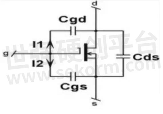
Fig.5
Using Equation (1) on the right voltage node, the following equation can be obtained:
I1 = CGD x d (VGS - VDS)/dt = CGD x (dVgs/dt - dVds/dt) (2)
I2 = CGS x d (VGS/dt) (3)
If the grid-source voltage VGS is applied to the MOSFET, the leak-source voltage VDS will drop (even in a non-linear fashion). Therefore, the negative gain of connecting the two voltages can be defined as:
Av= -VDS /VGS (4).
Substituting Equation (4) into Equation (2), we can get:
I1=CGD× (1+Av) dVgs/dt (5)
In the conversion (conduction or turn-off) process, the total equivalent capacitance Ceq of the grid-source electrode is:
IGATE = I1 + I2 = (CGD x (1 + Av) + CGS) * dVgs yet dVgs/dt = Ceq/dt (6)
The term (1+Av) is called the Miller effect, which describes the capacitive feedback between output and input in an electronic device. The Miller effect occurs when the grid-drain voltage is close to zero.
CDS diverts the most severe stage in a large area. Why? Because VD changes the most dramatically at this stage. It is precisely at this stage that the platform is formed. You can assume that the gate current IGATE is completely absorbed by the CDS and no current flows to the CGS.
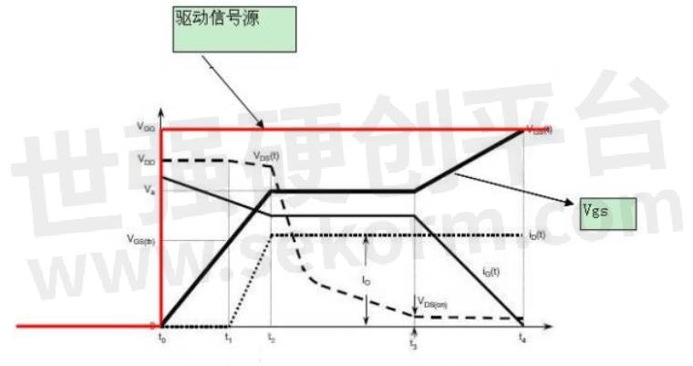
Fig.6
Note the representation in the datasheet:
CISS=CGS+CGD
COSS=CDS+CGD
CRSS=CGD
- +1 Like
- Add to Favorites
Recommend
- Details of MOS tube packaging
- The Differences between MOS Tube and IGBT Tube
- MOS Tube Drive Circuit Summary - Detailed Design of Various Switching Power Supply MOS Tube Drive Circuit
- Explain in Detail the Cause of MOS Tube Heating
- What is the Difference between MOS tube and IGBT?
- MOS Tube Knowledge, Must Read!
- How to Judge the Working State of MOS Tube?
- MOS Tube Anti-overvoltage Circuit
This document is provided by Sekorm Platform for VIP exclusive service. The copyright is owned by Sekorm. Without authorization, any medias, websites or individual are not allowed to reprint. When authorizing the reprint, the link of www.sekorm.com must be indicated.
Integrated Circuits


Discrete Components


Connectors & Structural Components


Assembly UnitModules & Accessories


Power Supplies & Power Modules


Electronic Materials


Instrumentation & Test Kit


Electrical Tools & Materials


Mechatronics


Processing & Customization


