Solve the mystery of MOS tube damage

Today, we share about solving the mystery of MOS tube damage.
1. Avalanche damage
Failure occurs when a breakdown voltage, V(BR)DSS (depending on the breakdown current), is applied between the drain and source electrodes beyond the rated VDSS of the device and a certain amount of energy. Avalanche failure can be caused by a back sweep voltage generated when a dielectric-loaded switch is running off, or by a mode in which the peak voltage generated by the leakage inductance exceeds the power MOSFET's drain-rated withstand voltage and enters the breakdown zone.
Typical circuit:
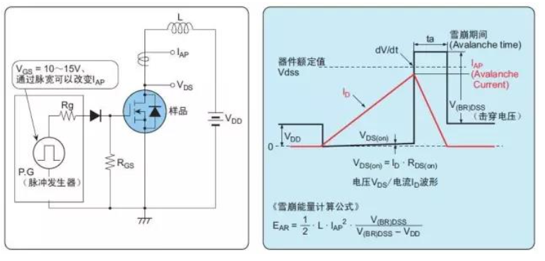
Fig.1
2. Device heating damage
Caused by a fever outside a safe area. The causes of heating can be divided into dc power and transient power. Dc power cause: Heating caused by loss of applied DC power
RDS(on) loss of on-off resistance (RDS(on) increases at high temperature, resulting in certain current current and increased power consumption)
Losses caused by leakage current IDSS (very small compared with other losses)
Cause of transient power: plus single trigger pulse
Load short circuit
Switch loss (on, off) * (related to temperature and operating frequency)
TRR losses of built-in diodes (short circuit losses of upper and lower bridge arms) (related to temperature and operating frequency)
The overcurrent caused by the load short circuit does not occur during the normal operation of the device, causing instantaneous local heat and resulting in damage. In addition, when the chip cannot dissipate heat normally due to heat mismatch or the switch frequency is too high, the continuous heating will cause the temperature beyond the channel temperature and lead to the destruction of thermal breakdown.

Fig.2
3. Internal diode damage
When the parasitic diode formed between the DS ends runs, this mode of diode failure is caused by the parasitic bipolar transistor running at MOSFET power at Flyback.

Fig.3
4. Damage caused by parasitic oscillations
This failure mode is particularly prone to occur in parallel.
Gate parasitic oscillation occurs when grid resistance is not inserted in parallel power MOS FET but connected directly. This parasitic oscillation occurs on a resonant circuit formed by gD-drain capacitor CGD(CRSS) and gate pin inductance Lg when the drain-source voltage is switched on and off repeatedly at high speed. When resonance conditions (omega = 1 L/C omega) were found, in the grid - the source electrode and is far greater than the vibration of the driving voltage VGS (in) voltage, due to beyond grid-rated voltage source electrode grid, or switching, disconnect the drain-source electrode voltage vibration voltage through the grid - drain capacitance CGD and VGS waveform overlap lead to positive feedback, so may be caused by misoperation oscillation.

Fig.4
5. Grid surge and electrostatic failure
There are mainly failures caused by voltage surge and static electricity between the gate and the source, namely gate overvoltage failure and gate failure caused by static electricity in the on-charge state at both ends of GS (including installation and electrification of measuring equipment).
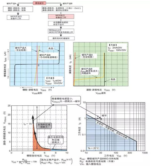
Fig.5
- +1 Like
- Add to Favorites
Recommend
- Details of MOS tube packaging
- The Differences between MOS Tube and IGBT Tube
- MOS Tube Drive Circuit Summary - Detailed Design of Various Switching Power Supply MOS Tube Drive Circuit
- Explain in Detail the Cause of MOS Tube Heating
- What is the Difference between MOS tube and IGBT?
- MOS Tube Knowledge, Must Read!
- How to Judge the Working State of MOS Tube?
- MOS Tube Anti-overvoltage Circuit
This document is provided by Sekorm Platform for VIP exclusive service. The copyright is owned by Sekorm. Without authorization, any medias, websites or individual are not allowed to reprint. When authorizing the reprint, the link of www.sekorm.com must be indicated.
Integrated Circuits


Discrete Components


Connectors & Structural Components


Assembly UnitModules & Accessories


Power Supplies & Power Modules


Electronic Materials


Instrumentation & Test Kit


Electrical Tools & Materials


Mechatronics


Processing & Customization


