Hardware Necessary Skills, MOS Tube Composed of Basic Gate Logic Circuit

This article shares the following key points:
OD gate is a very important concept of digital circuit, which is composed of a Buffer and drain open circuit.
Inverters, lines, and logic how to play, and how to use?
Apply typical circuits to understand basic logic gates, gates, or gates, and nongates, based on schematic diagrams and truth tables.
What about semiconductors SS, TT, and FF?
1. MOS tube logic circuit (and gate, or gate, non-gate, etc.)
As a hardware engineer, you can't help but understand chips. To understand the chip, the basic logic circuits composed of MOS tubes must be memorized to be able to understand the chip block diagram more proficiently. The field-effect Transistor provides a variety of gate circuits that can be visualized in a variety of combinations or visuals that, as described in the beginning, maybe the basis of a modern IC. The following circuit forms exist in a large number of commonly used 74 series chips, and the OD gate introduced later, buffers are commonly seen in the chip GPIO port and other pin designs.
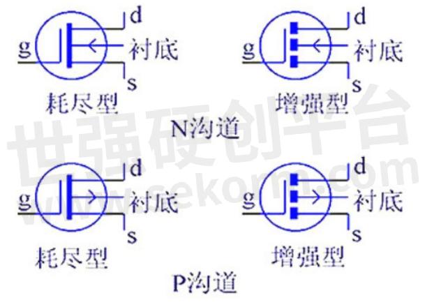
Fig.1
MOS tube constitutes the basic gate, or gate circuit
The door can be composed of six tubes, so the schematic diagram should be clearer to see the work diagram with the door, and then the truth table can see the corresponding relationship between the input and output. In this paper, the corresponding circuit with the gate is given. If you are interested, you can think about the circuit structure of the gate. There is a corresponding relationship between the two.
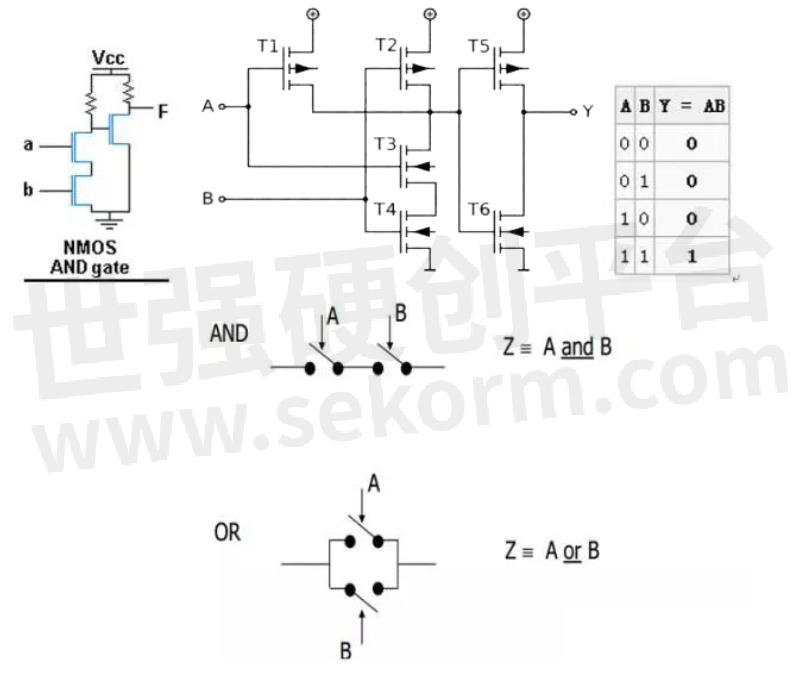
Fig.2
2. The inverter
The diagram below shows the circuit diagram of the inverter. The input and output states are opposite, which is called the inverter.
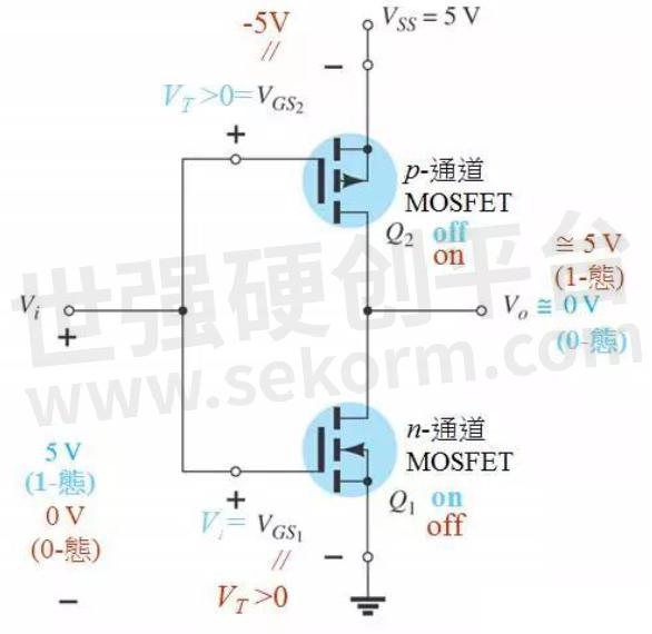
Fig.3
Circuit analysis:
The input Vi is low power, the upper tube is on, the lower tube is off, and the output is high level. The input Vi is high level, the upper tube is off, the lower tube is on, and the output is low level.
Nand gate:
The diagram below shows the circuit diagram of and not gate, which is equal to zero and different from one.
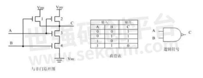
Fig.4
When A and B inputs are all at low power, 1,2 tubes are on and 3,4 tubes are off. The voltage at terminal C is consistent with VDD and the high level is output. When A inputs a high level, B inputs a low level, 1,3 tube conduction, 2,4 tube cutoff, the potential at the C end is consistent with the drain of 1 tube, output high level. When A inputs low level, B inputs high level, 2,4 conduction, 1,3 tube cutoff, C end potential, and 2 tube drain are consistent, output high level. When A and B inputs are all at high voltage, 1 and 2 tubes are off, 3 and 4 tubes are on, the voltage at the C terminal is consistent with the ground, and the output is low level.
4. Buffer
CMOS buffer (buffer), buffer, and inverter are the opposite, buffer input and output are the same, and inverter input and output are opposite.
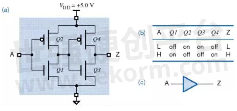
Fig.5
Circuit analysis:
The first stage Q1, Q2 constitutes an inverter; The latter stage Q3, Q4 constitutes a phase inverter, which is equivalent to inverting the phase twice, so it is reduced again.
5. Drain open door
Drain open door is a very classic circuit, commonly seen in the main chip GPIO port or single-chip GPIO port design. The most important point to note is that the open drain state is a high-resistance state, which generally requires a pull resistor.
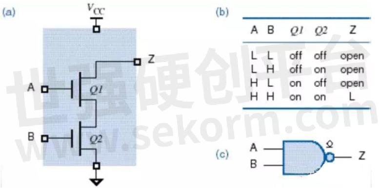
Fig.6(Application of drain Open Door - Line and Logic)Z=z1z2z3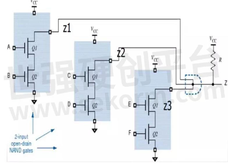
Fig.7
The reason for "line and" logic is that the audio output from multiple logic units shares a pull-up resistor. As long as one logic unit outputs a low level, that is, the collector (drain) opens output tube conduction, then the low level is output. Only all the units are cut off, and the output end is set to a high level by the pull-up resistor. This is a very practical circuit, which can be used in logic arbitration and other circuit systems.
Perhaps after a few years of work, the general will feel that the transistor circuit is very simple, which can only show that the research is not deep enough. Sometimes the simpler things are the more complicated things at the bottom. For example, from the point of view of technology, the transistor is divided into TT, SS, and FF, IC design is not around these, the basic is not easy, considering more in-depth, but I think only scratches the surface.
Fig.8
- +1 Like
- Add to Favorites
Recommend
- Details of MOS tube packaging
- The Differences between MOS Tube and IGBT Tube
- MOS Tube Drive Circuit Summary - Detailed Design of Various Switching Power Supply MOS Tube Drive Circuit
- Explain in Detail the Cause of MOS Tube Heating
- What is the Difference between MOS tube and IGBT?
- MOS Tube Knowledge, Must Read!
- How to Judge the Working State of MOS Tube?
- MOS Tube Anti-overvoltage Circuit
This document is provided by Sekorm Platform for VIP exclusive service. The copyright is owned by Sekorm. Without authorization, any medias, websites or individual are not allowed to reprint. When authorizing the reprint, the link of www.sekorm.com must be indicated.
Integrated Circuits


Discrete Components


Connectors & Structural Components


Assembly UnitModules & Accessories


Power Supplies & Power Modules


Electronic Materials


Instrumentation & Test Kit


Electrical Tools & Materials


Mechatronics


Processing & Customization


