Minimize Electromagnetic Interference and ESD Risks in Circuit Board Design

The ESD pulse follows a low impedance path. It is necessary to pay attention to the length of the line leading to the ESD protection diode and DUP, as well as the impact of the line diverging from the connector into two paths when considering the circuit board line inductance. If the circuit board circuit leading to the ESD protection diode has a high inductance, ESD energy will be injected into the DUP.
Figure 1: A comparison was made between a circuit with an ESD protection diode added near the DUP and a circuit with it placed near the connector. From this figure, it can be seen that when the ESD protection diode is placed near the connector, the first peak voltage is nearly 10V lower than when it is placed near the DUP.
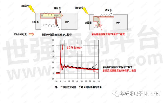
Figure 1
Therefore, the following key factors need to be considered in the circuit board design process:
1. Line length: The length of the line leading to the ESD protection diode and DUP must be carefully considered. Long line lengths may cause reflection and interference of high-frequency pulses, thereby affecting the protection effect.
2. Layout near the connector: Placing the ESD protection diode near the connector can effectively reduce the peak voltage during impact. This helps to quickly transfer voltage to the ground wire in the event of an ESD event, reducing damage.
3. Inductance impact: Consider the impact of the inductance of the circuit board circuit on ESD energy transmission. Excessive inductance may cause energy to be injected into other circuits, reducing protection effectiveness.
In Figure 2, a circuit board circuit that runs parallel to the external connection is shown. This layout may lead to some potential issues, especially when facing ESD events. When the lines on the circuit board run parallel to the lines connected to the outside, the following problems may occur:
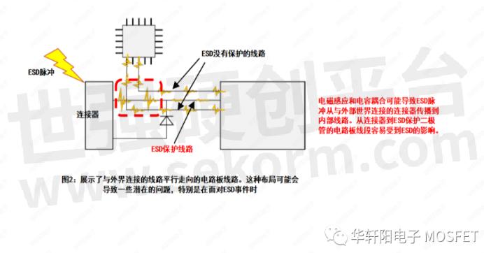
Figure 2
1. Electromagnetic interference: There is electromagnetic coupling between parallel lines, and when high-frequency signals are transmitted by external lines, it may cause electromagnetic interference in adjacent lines, thereby affecting the normal operation of the circuit.
2. Electrostatic discharge (ESD) propagation: If the external circuit is subjected to an ESD event, due to capacitive coupling between parallel lines, ESD pulses may propagate to the parallel circuit through capacitive effects, thereby affecting the internal circuit and causing damage or failure.
In order to reduce the impact of these issues, appropriate measures need to be taken during circuit board design:
1. Isolation spacing: When laying out circuit board circuits, consideration should be given to the isolation spacing between parallel circuits. Increasing the spacing between parallel lines can reduce the risk of electromagnetic coupling and ESD propagation.
2. Ground wire shielding: Adding a ground wire shielding layer near parallel lines can reduce the possibility of electromagnetic interference and ESD propagation. This helps to protect internal circuits from external interference.
3. ESD protection: Adding appropriate ESD protection measures between parallel lines and external connecting lines, such as ESD protection diodes, can prevent ESD pulses from spreading to internal lines and causing damage.
By adopting reasonable layout design and necessary protective measures, interference and risks between parallel lines and external connection lines can be minimized to the greatest extent, ensuring the stability and reliability of the circuit board.
In summary, circuit board layout plays a crucial role in ESD protection. Relying solely on high-performance ESD protection diodes is not enough, but also requires reasonable electrical.
Design circuit boards to optimize protection effects and reduce the impact of ESD events on the circuit. Therefore, in the design process, it is necessary to comprehensively consider factors such as line length, layout near connectors, and inductance to ensure that the circuit board can provide reliable protection in the face of ESD events.
- +1 Like
- Add to Favorites
Recommend
- Applied Power Microelectronics and Sekorm Announced a Distribution Agreement that Brings ESD, Surge Protection Devices, Diodes and More
- Bringing Power Supply Control ICs, TVS, ESD Electrostatic Protection Device and Other Products, TECHPUBLIC Announced a Distribution with Sekorm
- ESD Protection Diode Failure Modes and Precautions for Use
- YINT‘s ESD0524P ESD Protection Diode Design with Only 0.5mm Pitch to ESD Protection Circuits for HDMI
- Huaxianyang Electronics ESD/TVS Static Surge Protection Components - Your Trusted Choice
- Why Is JEDEC’s Maximum Requirement Of 30KV?
- Diotec‘s ESD5Z5V0 ESD Protection Diodes in the Tiny SOD-523 Protects Earphones Against Static Discharge
- Diotec‘s ESD Protection Diode ESD9L1P8 for Auto-Preserving Cookers
This document is provided by Sekorm Platform for VIP exclusive service. The copyright is owned by Sekorm. Without authorization, any medias, websites or individual are not allowed to reprint. When authorizing the reprint, the link of www.sekorm.com must be indicated.
Integrated Circuits


Discrete Components


Connectors & Structural Components


Assembly UnitModules & Accessories


Power Supplies & Power Modules


Electronic Materials


Instrumentation & Test Kit


Electrical Tools & Materials


Mechatronics


Processing & Customization


