New Gate-drive Techniques Reduces the Cost and Complexity of Implementing Sic Fet Designs in Ev Systems

Electric vehicles are pushing the limits of today’s power conversion technology, and the advent of high-power silicon-carbide (SiC) FETs has pushed the envelope even further. The many advantages of SiC FETs allow for higher switching speeds and higher voltages yielding smaller magnetics, lighter-weight cables, and higher efficiencies. These improvements have given electric vehicles a greater range and more capabilities.
New gate-drive techniques are required for SiC FET designs. One requirement is that they include negative gate voltages to ensure SiC FETs stay completely off. Generation of these negative voltages requires use of an isolated power supply. Thus the design of SiC gate drives may seem to be a daunting task. However, a review of half-bridge fundamentals and flyback converter techniques can quickly demystify the necessary steps in the design.
At the heart of the onboard chargers (OBCs), main dc-dc converters, traction inverters, and many other systems that make up EVs are two switching devices. They are typically depicted in schematics as being stacked one on top of the other, forming a half bridge. Half bridges allow the center node between the two switching devices to be efficiently pulled to the positive or negative rail. In an EV, these rails are typically the dc link rails which can reach 800 or even 1,000 V with the latest SiC FET technology. Unfortunately, stacking the FETs in a half- bridge configuration requires special attention to gate driver ground references.
To turn on a FET, the gate-source voltage, VGS, must be raised to a certain level, usually ~15 V for SiC FETs. Gate drivers typically pull the gate voltage to their VDD rail to turn on the FET. If the gate drivers use the same power rails, and the high-side gate driver’s ground is tied to the negative rail (dc link-), the output of the high-side gate driver is referenced to the dc link-. This ground connection creates many issues and simply does not work.
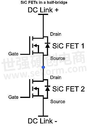
SiC FETs in a half-bridge configuration. Half bridges allow the center node, shown by the blue circle, to be efficiently pulled to the positive or negative rail. In an EV, these rails are typically the dc link rails, which can reach 800 or even 1,000 V with the latest SiC FET technology.
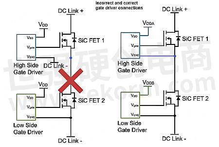
An incorrect gate driver connection (left) and a correct connection (right). If the gate drivers use the same power rails, and the high-side gate driver ground is tied to the negative rail (dc link -), the output of the high-side gate driver is referenced to the dc link. This creates many issues and simply does not work. For example, if the low-side FET is off, then the source of the high-side FET is floating relative to the high-side gate driver, and VGS is unknown. The solution: The two gate drivers use separate power supplies, and the high-side gate driver’s ground is tied to the source of the high-side FET.
For example, if the low-side FET is off, the source of the high-side FET floats relative to the high-side gate driver, and VGS is unknown. The solution: The two gate drivers use separate power supplies, and the high-side gate driver’s ground is tied to the source of the high-side FET. In this configuration, the high-side gate driver is referenced to the FET source connection; so, even as the FET source rises to dc link+, the gate-source voltage remains the same.
With the high-side gate drive issue solved, the next step is to generate power supplies for the gate drivers and negative gate voltage. The correct connection uses separate power supplies, and the high-side gate driver ground is tied to the high-side FET’s source.
The process of designing supplies for the gate drivers in a half bridge can often become a daunting endeavor involving dc-dc controllers, transformers, and PCB area constraints. The negative gate voltage requirement of SiC FETs further complicates supply design. Finally, most EV systems connect to the high-voltage dc link and require that the low-voltage control portion be isolated from the high-voltage power conversion stage. However, with a few upgrades, a flyback converter can be modified to meet all of these requirements.
Most EVs today have a main dc-dc converter that steps the dc link voltage down to the lower voltage rails (typically 12 and 48 V) used by most low-power electronic systems. By means of an isolated flyback converter, one of these low-voltage rails can be used to power the isolated gate drivers. In a typical configuration, a flyback converter’s transformer provides isolation and has two separate secondary side windings to create two supplies for the two gate drivers. Because the two outputs are coupled by the transformer, the dc-dc controller only directly regulates one of the two outputs.
The other output is indirectly regulated through the interwinding coupling of the transformer. This configuration causes the indirectly regulated output to perform slightly worse than the directly regulated output but not enough to impact the overall system. Use of a single transformer and converter for both outputs reduces board space and cost. By leveraging this configuration, the transformer can be further modified to create the negative gate voltage required by SiC FETs.

A half bridge with a dual-output flyback converter for powering isolated gate drivers. Here, the 12-V rail powers both the primary side and secondary sides of the isolated gate drivers. The flyback converter’s transformer provides isolation and has two separate secondary side windings to create two supplies for the two gate drivers. Because the two outputs are coupled by the transformer, the dc-dc controller only directly regulates one of the two outputs. The other output is indirectly regulated through the interwinding coupling of the transformer.
Now consider a flyback transformer modified to with taps in the middle of each of the two output windings (denoted VMIDA and VMIDB in the nearby schematic). In the high-side gate driver power domain, the middle tap creates a positive voltage relative to one of the end taps (VGNDA in the schematic) and a negative voltage with respect to the other (VDDA). The source of the high side FET is tied to the middle tap (VMIDA) and the gate driver remains referenced to the low tap (VGNDA). When the gate driver turns the FET off, it pulls the FET gate to its ground. This causes the voltage on the gate of the FET (VGNDA) to be below that of the source voltage (VMIDA) . The connection creates a negative gate voltage to ensure the SiC FET is held in the off state.
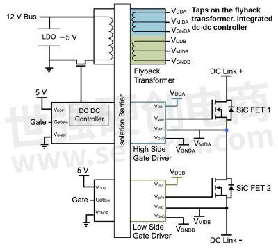
The flyback transformer modified with taps for VMIDA and VMIDB to the two output windings. In the high side gate driver power domain, highlighted in blue, VMIDA creates a positive voltage relative to VGNDA and a negative voltage with respect to VDDA. The source of the high side FET is tied to VMIDA, and the gate driver remains referenced to VGNDA. When the gate driver turns the FET off, it pulls the FET gate to its ground resulting in the voltage on the gate of the FET (VGNDA) going below the source voltage (VMIDA). Now a negative gate voltage ensures the SiC FET is held in the off state. Likewise, this same operation applies to the low-side gate driver power domain, highlighted in green.
Note this configuration also changes the gate-source voltage when the gate driver turns the high-side SiC FET on and pulls the FET gate to the high-side tap voltage (VDDA). Adjusting the transformer turns ratio between the middle tap and the high and low taps (VDDA to VMIDA and VMIDA to VGNDA) sets the middle-tap voltage (VMIDA). Likewise, this same operation applies to the low-side gate driver power domain.
Many isolated gate driver devices, such as the Silicon Labs’ Si828x, include a dedicated VMID pin to sense the drain-to-source voltage across the SiC FET for desaturation detection. To further reduce cost and board space, many isolated gate drivers include a built-in dc-dc controller. The Silicon Labs’ Si828x also includes this feature. The integrated dc-dc controller eliminates the need for a separate controller IC and often makes optocoupler feedback unnecessary because the isolated gate driver passes the feedback across the isolation barrier internally. Thus through use of a flyback converter with a sophisticated transformer design, a single dc-dc converter can power the isolated gate drivers and generate the negative gate voltage.
A sophisticated flyback converter coupled with the latest innovations in isolated gate drivers simplifies the task of driving SiC FETs in half-bridge configurations. It also reduces the cost and complexity of implementing SiC FET designs in the many EV systems using half bridges. As systems from onboard chargers to traction inverters adopt SiC FETs, electric vehicles gain higher efficiency, can work at higher voltages, and employ lighter-weight components, truly making them the automobiles of the future.
- +1 Like
- Add to Favorites
Recommend
This document is provided by Sekorm Platform for VIP exclusive service. The copyright is owned by Sekorm. Without authorization, any medias, websites or individual are not allowed to reprint. When authorizing the reprint, the link of www.sekorm.com must be indicated.
Integrated Circuits


Discrete Components


Connectors & Structural Components


Assembly UnitModules & Accessories


Power Supplies & Power Modules


Electronic Materials


Instrumentation & Test Kit


Electrical Tools & Materials


Mechatronics


Processing & Customization


