Knowles Microstrip Filter Helps Your Thin Film RF Devices to Achieve the Best Performance

As the demand for faster communications across consumer and commercial devices continues to increase, the operating frequencies of RF devices are being pushed higher and higher. This creates a number of challenges for RF device designers, as filter size must be reduced to compensate for smaller device sizes and shorter wavelengths while also maintaining high levels of performance. While surface mount technology (SMT), and in particular microstrip implementations, is an excellent option to meet these demands, it is important to note that not every SMT microstrip filter is created equal. There are a variety of choices to discuss with your filter suppliers, such as substrate type, plating technology, and topology that can dramatically reduce the size and increase the performance of an SMT microstrip filter. One particular choice that Knowles Precision Devices has guided customers through for decades is the decision to use thin film for these filters.

At a high level, a thin film is a layer of material used to fabricate electronic components that generally ranges from fractions of a nanometer to several micrometers in thickness. Since circuits constructed with the thin film are built using a distributed element structure created lithographically on a ceramic substrate, this brings the following advantages over other filter development techniques such as printing on PCBs:
High-precision patterning
Tight tolerance filter structures with less part-to-part variation and lower loss
The ability to develop components that are much more compact
In addition, by taking advantage of ceramic material properties to effectively slow a wave down, Knowles can shrink the wavelength to construct filters that are physically smaller than the signal’s wavelength in free space. Together, these characteristics make the thin film a particularly good material choice for high-frequency RF devices where precision and accuracy are essential. However, there are some challenges with this approach that must be carefully considered and addressed that Knowles will explore next.
Knowles Experts Help You Overcome the Challenges of Thin Film
To reduce circuit size and costs, most modern systems are not actively cooled. This means all the components in the circuit need to operate well over a wide range of temperatures, making temperature stability a key consideration for the thin film material selected. In short, the ceramic used in the thin film filter must be specifically designed to minimize variation in temperature. Guaranteeing temperature stability is an issue when using off-the-shelf materials like Alumina, but it is not a problem when working with Knowles Precision Devices because Knowles is vertically integrated from the raw material up. Knowles also designs all Knowles substrate ceramics to be temperature stable.
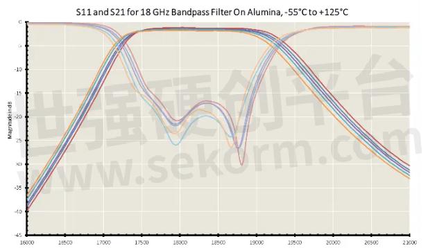
Additionally, Knowles has spent a lot of time testing microstrip filter temperature stability for a variety of substrates. In Figures 1 and 2, you can see an example comparison between two 18 GHz band-pass filter designs – one lot was manufactured on Knowles CF substrate and the other was done on an Alumina board. Knowles measured the filter response from -55℃ to +125℃.

Figure 1. Response of Microstrip Bandpass Filters on Alumina

Figure 2. Response of Microstrip Bandpass Filters on CF Dielectric
As you can see in the Figures above, the CF parts do not change very much, despite the wide temperature range. This is because Knowles custom ceramics are engineered with temperature stability in mind, which is very important if you need parts with reliable, predictable performance over a range of operating temperatures.
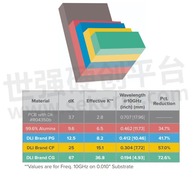
Another challenge of working with thin film today is how much size reduction can be achieved. Again, with Knowles engineered ceramics Knowles can design devices that are substantially smaller than those built on Alumina.

Figure 3. A comparison of two common substrates to three Knowles Precision Devices custom ceramics.
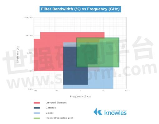
It’s clear that filters designed using thin film have several key advantages, especially for RF devices operating at high frequencies. But to fully utilize these advantages, you need to be careful about the material properties of your selected substrate. For Knowles Precision Devices, thin film development is nothing new as we provide a variety of bandpass, lowpass, and highpass filters from 1GHz to 42GHz (and beyond) using our thin-film microstrip technology as shown in Figure 4.

Figure 4. The frequency range covered by Knowles microstrip filters is shown in the green area.
Knowles is well prepared to not only guide customers through the substrate selection process, but Knowles expert material scientists have developed a number of custom ceramics for thin film development that offers significantly better thermal performance than most industry-standard ceramics. Plus, Knowles thin film substrates have a sufficiently higher dielectric constant (K) that is ideal for miniaturization and temperature-stable performance. This makes Knowles custom ceramics a much better option for temperature stability than off-the-shelf substrates like Alumina. Knowles customers can also develop substantially smaller RF components than if they were to use Alumina.
- +1 Like
- Add to Favorites
Recommend
- Knowles‘ Microstrip Filters Offer a High Repeatability and Temperature Stability from -55℃ to 125℃
- The Anatomy of a Microstrip Isolator and Circulator: Understanding the Basics of Microwave Microstrip Isolator and Circulator Technologies
- Microstrip Isolator/Circulator Mounting Instruction Manual
- Planar Filters Continue to Advance
- The Pros and Cons of Different Filter Structures
- High Performance Microstrip Circulators Embedded into The Active Antenna Transmitter/receiver Modules for Thales Alenia Space
- Switch Filter Banks for Agile RF Receiver Design in Radar
- Knowles to Participate in Upcoming Baird Conference in New York on June 4, 2024
This document is provided by Sekorm Platform for VIP exclusive service. The copyright is owned by Sekorm. Without authorization, any medias, websites or individual are not allowed to reprint. When authorizing the reprint, the link of www.sekorm.com must be indicated.


