Knowles‘ Microstrip Filters Offer a High Repeatability and Temperature Stability from -55℃ to 125℃

Since Knowles acquired Integrated Microwave Corporation (IMC) in 2020, Knowles has an extended its range of RF and microwave filtering solutions to include a wide variety of ceramic coaxial resonators, lumped element filters, and cavity filters from the VHF to the Ka-band. During this time, Knowles has continued to innovate and expand product offerings for one of the most popular filter types – the Microstrip Filter.

If you are not familiar with microstrip technology, it was first released in 1952. Since then, numerous advancements in dielectric material manufacturing and thin film processing techniques have led to the adoption of microstrip filtering for a wider range of applications, especially at mmWave frequencies.
An Overview of How Microstrip Technology Works
At a high level, microstrip refers to a type of planar transmission line technology that consists of a conducting strip separated from a ground plane by a dielectric substrate as shown in Figure 1.

Figure 1. A diagram of a typical microstrip filter configuration.
More specifically, the design and construction of a microstrip filter are similar to the way circuits are configured on a printed circuit board (PCB). However, a key distinction of a microstrip filter is that the metal conductor patterns printed on the solid dielectric substrate are there to create resonators rather than just interconnects. The metal circuit patterns of strip elements are placed on a solid dielectric insulating layer with a metal ground layer below the dielectric. The fields surrounding the strip permeate two different media, with part of the field in the substrate and another in the air the strip. The higher permittivity of the dielectric substrate causes the electric field to concentrate in the substrate, which means field losses due to material choice become a factor. Standard PCB materials like FR4 can be used below 1GHz for low Q filters. Lower loss and increased Q can be achieved using ceramic materials.
This type of printed transmission line is a popular filtering option since these filters can cover a broad frequency range, are economical to produce, and are often lighter and more compact than alternative transmission line technologies such as waveguide.
Overcoming Issues with Loss for Microstrip Filters
The biggest concern with microstrip filters is the loss experienced compared with other transmission-line and waveguide filtering approaches. However, the evolution of high-k materials, such as PG, CF, and CG ceramics, is making it possible for RF engineers to develop low-loss microstrip transmission-line filters.
In Figure 2, Knowles shows how a microstrip transmission-line configuration using Knowles PG ceramic reduces loss compared to a microstrip filter using a common RO4350 LoPro dielectric. In this comparison, Knowles used the same material thickness, metal conductivity, and 50-Ω microstrip transmission line in both configurations.
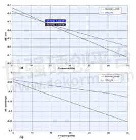
Figure 2. Plot A illustrates loss/inch and plot B shows loss/wavelength.
Beyond loss reduction, when a filter manufacturer also engineers the substrate material, this offers another key benefit – the ability to substantially shrink the wavelength of the electromagnetic waves propagating along a microstrip transmission line. For a microstrip line, the wavelength is determined using the following equation:
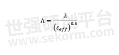
Λ = Wavelength in microstrip
λ = The free-space wavelength
εeff = The effective dielectric constant, which depends on the dielectric constant of the substrate material and the physical dimensions of the microstrip line.
Let’s look at the Knowles catalog surface mount bandpass filter the B099NC4S, which is a popular X band filter, as an example. This filter has dimensions of 10.2mm x 3.8mm, or in terms of free space wavelength at 12GHz, 0.4λ x 0.15λ. We can use the material advantages we achieve by developing Knowles' substrates to shrink the wavelength inside the filter (per the equation above) so that the filter ends up quite small compared to any radiation outside the filter – i.e. in free space.
This also means we can develop small-scale microstrip surface mount technology that is ideal for mmWave applications. And since we can make the physical size of antennas at mmWave frequencies sufficiently small, it makes sense to build complex antenna arrays on chips or the PCB directly using a microstrip approach. Therefore, entire devices including antennas, couplers, filters, and power dividers can be formed by creating metalized patterns on the substrate.
The Capabilities of Knowles Microstrip Filters
Knowles Precision Devices provides a variety of bandpass, lowpass, and highpass filters from 1GHz to 42GHz (and beyond) using thin-film microstrip technology as shown in Figure 3.

Figure 3. The frequency range covered by Knowles microstrip filters is shown in the green area.
All Knowles microstrip filters offer the following key benefits:
Temperature stability from -55℃ to 125℃
A reduction in filter size versus using a typical PWB of up to 20x using Knowles CG material, 10x using CF, or 3x using PG
High repeatability since thin film manufacturing provides precise manufacturing performance with no tuning required
Knowles also has the in-house expertise to develop custom microstrip filters for higher frequency ranges.
- +1 Like
- Add to Favorites
Recommend
- Knowles Supertweeters Power New EarSonics Precision In-Ear Monitors
- Knowles to Participate in Upcoming Baird Conference in New York on June 4, 2024
- Knowles Extends Custom Miniaturization Capabilities to MedTech OEMs
- Knowles Introduced the MD Series, A Range of Medical-grade Capacitors for Implantable Designs
- Knowles Partners With Ole Wolff to Deliver Compact Hybrid Driver for TWS Earphones With HD Audio and ANC
- Knowles 3-Cell Supercapacitors Support Significant Jump in Energy Storage
- Knowles and Meizu Bring Treble Performance to New Heights with LIVE AI Noise Cancelling Hi-Fi Earbuds
- Knowles Microstrip Filter Helps Your Thin Film RF Devices to Achieve the Best Performance
This document is provided by Sekorm Platform for VIP exclusive service. The copyright is owned by Sekorm. Without authorization, any medias, websites or individual are not allowed to reprint. When authorizing the reprint, the link of www.sekorm.com must be indicated.
Integrated Circuits


Discrete Components


Connectors & Structural Components


Assembly UnitModules & Accessories


Power Supplies & Power Modules


Electronic Materials


Instrumentation & Test Kit


Electrical Tools & Materials


Mechatronics


Processing & Customization


