UnitedSiC Rediscovers The Perfect Switch with SiC FETs

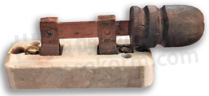
It's sometimes funny how things improve or worsen depending on your perspective. The perfect switch existed from the day electricity was harnessed – at least 18th-century experimenters such as Volta thought so when they fabricated an electrical isolator out of brass, wood, and porcelain. It had virtually no resistance when closed and no leakage when open. It could withstand as high a voltage as you like depending on how big you made it. It was a problem solved.
Semiconductors were a step back from the ideal
The first electronic switches, vacuum tubes, were large, lossy, and fragile, and early transistors were a further step backward, with high resistance and low breakdown voltage except, of course, you could flip them a lot faster than anything mechanical. They were small but consequently could only handle tiny currents. In the 75 years since Shockley and his team made their discoveries, engineers have worked to get back to Volta's ideal solution, but with pressure at the same time to switch ever faster at MHz rates, keep the small size and increase current rating.
The application that drove the development of transistors to higher power levels was of course the switched-mode power supply, which allowed the possibility of DC-DC power conversion without motor-generator sets and at high efficiency. The SMPS idea was patented in 1959 and bipolar junction transistors were used in the first commercial application in 1970, in the Tektronix 7000-series oscilloscopes. BJTs were successful in the application, but at higher powers were difficult to drive efficiently and switching losses were unacceptable at anything other than a few tens of kHz. Fast and easy-to-drive MOSFETs were patented as early as 1960, but early versions had significant on-resistance, producing high power loss at high currents due to the square term is I2R. A breakthrough, however, was the invention of the IGBT, with the ideal combination of an easy MOSFET gate drive and the on-state characteristics of a BJT, and, to this day, it remains a practical solution for very high-power converters. 'Practical' is not ideal though – to avoid unacceptable dynamic losses in the highest power applications, an IGBT's switching frequency must be kept below about 10KHz, mandating the use of large, heavy, and expensive magnetic components. In the meanwhile, MOSFETs switching at up to around 500kHz have improved to the latest state-of-the-art super-junction types which now dominate the low and medium power ranges of DC-DC and AC-DC conversion.
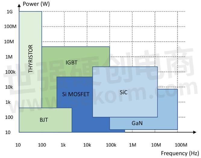
The approximate application areas of modern power semiconductors
In a bid to close the gap between IGBT and silicon MOSFET application areas, wide band-gap semiconductors have been explored, in silicon carbide and gallium nitride. These promise lower switching and conduction losses, stemming from better electron mobility values and higher dielectric withstand rating of the materials, enabling smaller devices with lower capacitances and conduction channel lengths. Manufacturing switches with the new materials has thrown up many difficulties though, from mismatched thermal expansion coefficients using practical substrates with GaN HEMT cells to lattice defects and basal plane dislocations in SiC MOSFETs, all degrading performance and reducing reliability. Refinements in fabrication continue to improve performance however and the devices, particularly SiC MOSFETs, are now mainstream and are encroaching into the traditional IGBT high-power applications.
Wide band-gap devices are a step back in some ways
In some ways, however, steps back have been taken; SiC MOSFETs and GaN HEMT cells are not as easy to drive as silicon MOSFETs, the required gate voltage levels are critical for optimum performance and reliability, and for SiC, the threshold exhibits wide variation and hysteresis. The reliability of the SiC MOSFET gate oxide has also been questioned and Gan HEMT cells have no avalanche rating, forcing heavy voltage derating. Another retrograde step is the performance of the devices when conducting in reverse by commutation, the automatic reversal of current caused by an inductive load – SiC MOSFETs have a body diode dropping around 4V under forwarding bias and with appreciable reverse recovery loss when subsequently reverse biased. When GaN devices commutate, they conduct through the channel with no reverse recovery issue, but voltage drop is again quite high and varies depending on gate drive.
Looking back to go forwards
A step in the right direction is to look back to an old technique – 'cascading silicon MOSFET and a SiC JFET, dubbed a 'SiC FET' by the manufacturer and technology champion UnitedSiC. It has better figures of merit for overall losses than SiC MOSFETs or GaN HEMT cells, the gate drive is non-critical with a stable threshold, the body diode is fast with low recovery loss and only around a 1.5V drop. Additionally, the devices have robust avalanche and short circuit ratings, independent of gate drive. Devices are available in 650V, 750V, 1200V, and 1700V classes, with on-resistances down to 7 milliohms in a variety of packages, with the majority of parts AEC-Q101 qualified, to allay any possible reliability concerns.
What's more, the challenges created by very fast and high speed switching with these devices can be solved by a simple RC snubber to manage turn-off overshoots and ringing and get the best performance out of these SiC FETs.
Is the perfect switch in view yet? Designers will always want improvements but we are surely very close with SiC FETs.
- +1 Like
- Add to Favorites
This document is provided by Sekorm Platform for VIP exclusive service. The copyright is owned by Sekorm. Without authorization, any medias, websites or individual are not allowed to reprint. When authorizing the reprint, the link of www.sekorm.com must be indicated.
Recommend

The totem-pole PFC stage comes of age with SiC FETs
2022-05-11 - Manufacturer News The gate drive issue is solved by designing with SiC FETs from UnitedSiC, a cascode combination of a SiC JFET and a silicon MOSFET. The gate now can be driven at ‘normal’ MOSFET or IGBT levels with a large margin of safety to the absolute maximum +/- values, with a stable threshold level when driving the device fully on, largely independent of time and temperature.
UnitedSiC‘s FET-Jet Calculator Taking The Guesswork out of SiC FET Selection
2021-07-11 - Manufacturer News UnitedSiC‘s new FET-Jet CalculatorTM is free-to-use without any registration and enables a designer to select an application, topology, electrical design parameters and ambient temperature, and quickly try a device from UnitedSiC‘s range of SiC FETs and diodes with a chosen heatsink rating. Critical performance results are instantly calculated, including overall efficiency, with component losses separated out into dynamic and conduction contributions, along with junction temperatures and current stress levels. If a resulting voltage is above the rating of the selected part, a warning is given.
UnitedSiC’s Web-based FET-Jet Calculator ——Makes Selection of A SiC FET and SiC Schottky Diode for Your Power Design
2021-11-26 - Manufacturer News If you haven’t found it yet, UnitedSiC’s free-to-use web-based FET-Jet calculator has been a revelation – it makes selection of a SiC FET and SiC Schottky diode for your power design a breeze.
SiC FETs save large energy for data centre
2020-06-18 - Application solution Article Designers might like to work from a blank sheet of paper when trying to solve the complex systemic optimisations involved in building a more energy-efficient data centre. The reality for many, though, will be to make many small improvements to what already exists. For power-supply design, UnitedSiC offers a range of SiC FETs in the widely used DFN8x8 package. The devices’ stacked cascode topology means they can be driven like a silicon MOSFET but will switch faster and handle more power, simplifying circuit design.

1200V Gen 4 SiC FETs with industry-best performance deliveroptimal SiC power solutions to high-voltage markets
May 2022 - Supplier and Product Introduction
UF4SC120030K4S,UF4C120053K3S,UF4C120030K4S,UF4SC SERIES,UF3C120040K4S,UF4C SERIES,UF4C120070K3S,UF4C,UF4C120070K4S,UF4C120053K4S,UF4SC120023K4S,UF4SC
UnitedSiC Announces 6 New SiC FETs, Available in 30/40/80/150mΩ Versions
2021-06-08 - New Product Introduction UnitedSiC, a leading manufacturer of silicon carbide (SiC) power semiconductors, continues to expand its FET portfolio with the introduction of six new 650V and 1200V options, all housed in the industry standard D2PAK-7L surface mount package. Available in 30, 40, 80 and 150mΩ versions, these latest SiC FETs represent another step forward in accelerating migration to SiC across applications such as server and telecom power supplies, industrial battery chargers and power supplies, EV on-board chargers and DC-DC converters.
UnitedSiC Introduces the Industry‘s First 750V SiC FETs Based on Advanced Gen 4 Technology
2021-01-11 - New Product Introduction December 1, 2020: UnitedSiC has launched the first four devices based on its advanced Gen 4 SiC FET technology platform. As the first and only 750V SiC FETs currently available on the market, these Gen 4 devices enable new performance levels. Available in 18 and 60 mohm options, these new SiC FETs deliver unmatched FoMs with reduced on-resistance per unit area, and low intrinsic capacitance.
SiC FETs, SiC JFETs and SiC Schottky Diodes Product Selector Guide
Product introduction SiC FETs SiC JFETs SiC Schottky Diodes
2022/4/22 - Selection guide UJ3D06506TS,UJ3D1220KSD,UF3C065040T3S,UF3C120080K3S,UF3C065040B3,UJ4C075023K3S,UJ3D1210KS,UF3N090350,UF3C SERIES,UJ3C065080B3,UJ3C120040K3S,UJ3N1701K2,UF3N SERIES,UJ3N065025K3S,UJ3N065080K3S,UF3SC120016K3S,UF3C065080K3S,UJ4SC,UF3N170400,UF3C065030K4S,UF3N120140,UF3N065600,UF3N170400B7S,UJ3D06510TS,UJ3D06560KSD,SC SERIES,UJ3C065030B3,UJ3D1210K2,UF3SC065007K4S,UF3C120400K3S,UJ4SC SERIES,UF4C120053K4S,UJ3C120150K3S,UJ4C075060K4S,UJ3D1202TS,UF3C065080B7S,UJ3D1220K2,SC,UF3C065080T3S,UF3C065040K3S,UJ3C120080K3S,UF3SC,UF4C120053K3S,UF3C120080K4S,UF3N090800,UJ4C075018K3S,UJ3D1210TS,UF3SC065030B7S,UJ4C075023K4S,UJ3D06530TS,UJ4C075060K3S,UJ3N SERIES,UJ3N120035,UF4C120070K3S,UF3SC120040B7S,UF3SC120016K4S,UJ4C SERIES,UJ4C075018K4S,UJ3C065080T3S,UF4SC120030K4S,UJ3N120035K3S,UJ3D06504TS,UJ3C065030K3S,UJ3D1205TS,UF3C065080B3,UJ3N065080,UJ4SC075009K4S,UJ3N120070K3S,UJ4C075033K3S,UF3SC SERIES,UF4C120070K4S,UF3C065030T3S,UJ3D06508TS,UJ3D1210KSD,UJ3D06516TS,UJ3D06512TS,UJ3D1250K2,UJ4SC075006K4S,UF3C120040K4S,UF3C065030B3,UF3C120150B7S,UJ3C SERIES,UF3C065040K4S,UJ4C075044K3S,UJ3C065030T3S,UJ4C,UJ3C120070K3S,UF3C065030K3S,UF4C,UJ3D1250K,UJ3D06520TS,UF3SC120009K4S,UF4C SERIES,UJ3N065025,UF3C120080B7S,UF3C120040K3S,UF3C120150K4S,UJ3C065080K3S,UJ3D1725K2,UJ3N120065K3S,UJ3D,UJ4C075044K4S,UJ3C,UJ3D06520KSD,UF3N065300,UF3C,UF3N,UJ3N120070,UJ4SC075011K4S,UJ4C075033K4S,UJ3N,UF3C170400K3S,UF4SC120023K4S,UJ3D SERIES,UF3SC065040B7S,UF3C065080K4S
Switching Characteristics of UnitedSiC Gen 3 SiC FETs at Elevated Temperatures APPLICATION NOTE
July 2019 - Application note & Design Guide
UF3C120040K4S
UnitedSiC (now Qorvo) Announces 1200V Gen 4 SiC FETs with Industry-best Figures of Merit
2022-05-19 - New Product Introduction UnitedSiC announced the new 1200V Gen 4 SiC FETs with industry-leading figures of merit in on-resistance.
SiC FETs are enablers for more efficient motor drives and faster charging
2020-06-28 - Application solution Article EV uptake is set to increase but ‘range anxiety’ and charge times are still barriers to general acceptance. Wide bandgap semiconductors are enablers for more efficient motor drives and faster charging and new SiC FETs are best performers.Current best-in-class devices from UnitedSiC are achieving under 7 milliohms on-resistance in 650V devices and under 10 milliohms for 1200V types that might be used in 480VAC line systems for the highest power chargers.
UnitedSiC SiC FETs: Industry’s lowest RDS(on) devices
Supplier and Product Introduction
UF3SC65007K4S,UF3SC120016K4S,UF3SC,UF3SC120016K3S,UF3SC120009K4S,UF3SC065007K4S
Regenerative power efficiency is becoming a real differentiator
2021-11-27 - Design Article IGBTs had a conduction loss advantage at the expense of significantly higher turn-off switching loss. SiC FETs have been steadily displacing IGBTs because they offer both lower switching and conduction losses.

Electronic Mall
 Auth. Dist.
Unit Price:$119.0770
Auth. Dist.
Unit Price:$119.0770
 Auth. Dist.
Auth. Dist.
Auth. Dist.
Auth. Dist.
Auth. Dist.
Auth. Dist.
Auth. Dist.
Auth. Dist.
Auth. Dist.
 Auth. Dist.
 Auth. Dist.

Integrated Circuits


Discrete Components


Connectors & Structural Components


Assembly UnitModules & Accessories


Power Supplies & Power Modules


Electronic Materials


Instrumentation & Test Kit


Electrical Tools & Materials


Mechatronics


Processing & Customization


