How GaN is Revolutionizing Motor Drive Applications

Rethinking the Ordinary and Overcoming Mental Biases
Motor drive applications span several markets: industrial, appliance, and automotive. A commonality that occurs regardless of market is that when a new technology is proposed, it faces resistance to its adoption; after all, it is human nature to stick with what is known and resist change.
It is happening now -- GaN technology is a game-changer for motor applications. The resistance to a new technology manifests as scare tactics from competitors of design complications, reliability concerns, and, specifically, in the case of motor drives, safety, and EMI challenges. In this post, I will dispel these myths and show why GaN is revolutionizing motor drive applications.
Effect of CRSS in Switching: How to Get Motor-Friendly dv/dt with GaN
When dealing with new technologies, such as the latest MOS, GaN, and SiC devices, it is quite normal to get switches that are faster than previous generations. It is a common bias to think that because a GaN device switches so fast, that the gate driver cannot maintain control. In reality, when looking closer at a given device, it is essential to consider its reverse capacitance (CRSS) characteristics, its linearity, and the ratio between its low voltage value and its high voltage value (CRSSslow/CRSShigh).
Conventional gate driving is done by applying a voltage to the gate of the switch through a resistor. If the value of the ratio CRSSlow/CRSShigh is too high, either of the following conditions can occur:
1.the switch is too fast at the beginning of the turn-on event, leading to high dv/dt
2.the switch is too slow at the end of the turn-on event, leading to a tail effect and higher power dissipation
This is embedded in the multi-segment nature of the CRSS curve.
So, how do silicon and GaN compare in reality?
Silicon: A typical 100 V MOS (BSC027N10NS5) has CRSSlow/CRSShigh = 1500 pF/35 pF = 43
GaN: The corresponding EPC 100 V eGaN® FET, an EPC2022, has CRSSlow/CRSShigh = 300 pF/6 pF = 50
Therefore, the eGaN FET can be slowed better than the MOS counterpart while keeping a lower switching dissipation. Also, the commutation waveforms of GaN are smoother because the CRSS curve is more linear than the MOSFET. An added advantage is that there is no reverse recovery from any intrinsic body diode, which further reduces EMI and acoustic noise.

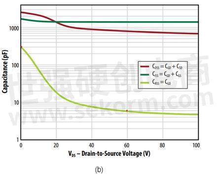
Figure 1: Capacitance vs. voltage for (a) BSC027N10NS5 MOSFET and (b) EPC2022 eGaN FET. The ratio of CRSS(low)/CRSS(high) as measured at 0 V and 60 V is 43 for the MOSFET and 50 for the eGaN FET.
Effect of dv/dt on Radiated EMI
The dv/dt can be slowed in a GaN inverter to reach each customer's needs. The question then becomes; what is the target? In high voltage motor applications (i.e., 320 V DC bus and higher), it is a common requirement to have less than 5 V/ns for insulation reliability.
Despite this limit, in the past companies I worked with, we successfully released FredFET and SuperJunction MOS-based smart modules switching at 15 V/ns. Those parts are sold in millions today and are widely accepted by motor drive customers.
But what about low voltage (i.e., 48 V) motors in battery-operated applications? There is no similar dv/dt target, and 10 V/ns to 20 V/ns is quite typical. It is a dv/dt target successfully reached by the GaN inverter without compromising the switching dissipation.
But is dv/dt an accurate predictor of radiated EMI? The answer is yes and no. Having spent many hours in EMC anechoic chambers, I can say that it is difficult to predict the EMI behavior of a drive by merely looking at dv/dt.
A common "wisdom" that the fast rise and fall times of GaN generate EMI is clearly not true, as is well known by people who work with hardware.
But is there any advantage in having the fastest allowed dv/dt in a motor application?
In reality, the fastest allowed dv/dt enables eliminating the dead time, which is no longer needed when dealing with GaN inverter.
Effect of Short Dead Time in Motor Inverters
Using a GaN inverter, it is possible to reduce dead-times to 10 ns or less, and hence apply a voltage to the motor that has lower harmonic distortion than in a MOS inverter with a dead-time of 200 ns or more. The superior linearity of the GaN inverter allows the lowest acoustic noise operation, especially at low speed. Moreover, the lowest harmonic content of the applied voltage is reflected in a lower harmonic distortion on the motor's current. Thus, a GaN inverter with no dead time leads to fewer vibrations, less heat, and less EMI.
The GaN Advantage When Increasing PWM Frequency in a Battery-operated Motor Inverter
A GaN inverter can be easily operated at 100 kHz PWM frequency thanks to its lower switching dissipation and smoother switching at the allowed dv/dt. An immediate result is that voltage and current ripples at the battery cables are drastically reduced, so there is no need for any LC input filter based on an electrolytic capacitor. A simple ceramic 22 uF capacitor with a low capacitance value can replace one 330 uF (or sometimes two) bulky electrolytic capacitors, thus saving costs, increasing efficiency, reliability, and lifetime.
The 100 kHz frequency range is where ceramic capacitors exhibit the lower ESR. At 100 kHz, ceramic capacitors are the best decoupling companion for GaN inverters.
Some Real Measurements on the EPC9146 Evaluation Board
In my lab, I ran the EPC9146 eval board, using the EPC2152 ePower™ Stage IC without filters, and measured 15 V/ns dv/dt in the fastest commutation at motor terminals. The dead time could be reduced to 10 ns, and the PWM frequency increased from 20 kHz to 100 kHz, enabling lower voltage and current ripple on the battery cables using 22 uF ceramic capacitors at 100 kHz when compared to one electrolytic 330 uF at 20 kHz.
Conclusion – GaN is On the Road of Innovation
As the adoption of GaN devices continues to accelerate, incumbent MOSFET producers recognizing that their products are nearing irrelevance, generate scare tactics to encourage designers to stick to the ordinary habit of doing things as they have always been done. However, the promised benefits of GaN are easily achievable in actual circuit design. With devices that are smaller, faster, reliable, and comparably priced, it is becoming increasingly difficult to find reasons not to use GaN FETs and ICs – it is a technology on the road to innovation!
- +1 Like
- Add to Favorites
Recommend
- Sharge Selects GaN FETs EPC2218 from EPC for High-power USB PD Charger Retro 67 to Achieve the Most Efficient Power Conversion
- Sekorm Became an Authorized Distributor of EPC(Efficient Power Conversion), Which Brings GaN FET Products
- 65A ePower™ Chipset from Efficient Power Conversion (EPC) Redefines Power Conversion
- Efficient Power Conversion to Showcase how GaN is Transforming Power Delivery and Enabling Advanced Autonomy Across Multiple Industries at PCIM 2022
- EPC Introduces EPC9157 48V to 12V Demo Board Featuring EPC eGaN FETs and New Renesas DC-DC Controller
- Efficient Power Conversion (EPC) Expands 100 V eGaN FET Family Offering Designers Best-in-Class Performance and Cost for 48 V DC-DC Conversion
- EPC‘s New EPC9165 Bidirectional Converter that Delivers 2kW with 96.8% Peak Efficiency
- GaN Power Components Will Be Cheaper Than Silicon Ones, Says EPC
This document is provided by Sekorm Platform for VIP exclusive service. The copyright is owned by Sekorm. Without authorization, any medias, websites or individual are not allowed to reprint. When authorizing the reprint, the link of www.sekorm.com must be indicated.
Integrated Circuits


Discrete Components


Connectors & Structural Components


Assembly UnitModules & Accessories


Power Supplies & Power Modules


Electronic Materials


Instrumentation & Test Kit


Electrical Tools & Materials


Mechatronics


Processing & Customization


