How To Use An EPC Development Board to Evaluate The Performance of A Given GaN FET or IC in Common Applications?

EPC development boards offer the opportunity to evaluate eGaN® FETs and ICs in common applications. For example, the EPC9094 half-bridge development board can be configured as a buck or boost converter. The EPC9094 features the newly released EPC2054 200V 43mOhm max eGaN FET in a 1.3 x 1.3 mm 2 x 2 pin WLCSP package. The very low RDS(on) value of this very small FET permits it to support high current loads from a high voltage supply. To demonstrate this ability, EPC will modify the EPC9094 development board to a buck converter. Using a 140V supply, Spice simulation suggest 28V output at 2.5A will offer a high 90% efficiency. A Vishay IHLP-4040DZET330M11, 33μH, 4.4A, 95mOhm Max, 10.2 x 10.8 x 4mm inductor is selected which will provide 40% ripple at 500kHz. Output capacitors consisted of four 10uF Y5V 50V 1210 ceramic capacitors. The simulation showed a tradeoff between ripple current and overall efficiency when switching frequency was changed between 500kHz down to 375kHz. The simulation also showed that adjusting the dead time to permit full ZVS transition from high to low maximized the light load efficiency performance in the buck converter.
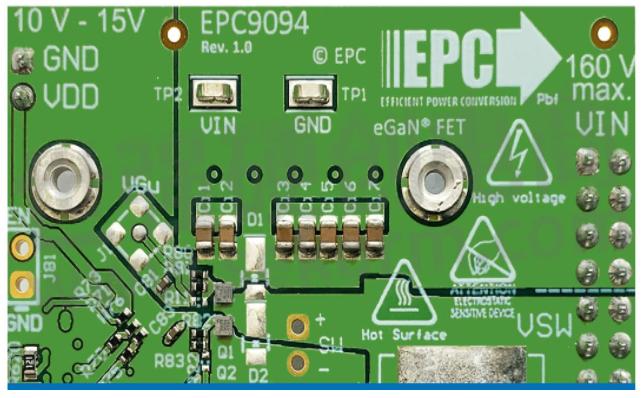
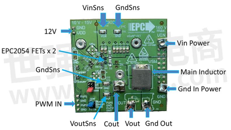
Figure 1: EPC9094 Development Board
Looking at the EPC9094 development board in Figure 1, there are multiple configuration options and connections. Power in is on the right and Power out is on the bottom. The board includes input voltage bulk capacitance. There is space to solder a large inductor and the output capacitors of your choice. Voltage sense points are offered for both input and output to permit high accuracy efficiency measurements. Additional pin-based connections are provided for gate driver bias power and PWM signal inputs. Finally, there are two jumpers offering three settings each. The blue jumper configures the board for Buck or Boost from a single PWM input or dual or independent high and low side FETs PWM inputs. The red jumper configures the dead time options.
1) No Bypass permits the development board's built-in dead time generators to function allowing customizable asymmetrical dead time for high and low side FETs.
2) DT Bypass means the development board's dead time circuit is deactivated.
3) Full Bypass reroutes both PWM input directly to the gate driver inputs with no signal processing delays.
The latter mode specially allows this development board to take advantage of the On-Semi's NCP51810/20 high voltage half bridge gate driver built in deadtime generator which is what we will use in this demonstration. Finally, there are three screw mounting studs of the correct height to allow for the optional attachment of a heatsink with TIM material to the top side of the EPC2054 FETs which would greatly extend the FET power handling range.
EPC's development boards do not come with traditional power terminals. However, banana jacks can easily be soldered to the terminals as shown in Figure 2. For the 12 V bias and the PWM pin input, hook clips can be used. BNC to hook clips adapters are available to make it easy to connect a pulse generator.
Figure 2: EPC9094 Connections
Figure 3 shows the switching waveform for the buck converter operating at full 2.5A load at 28V output. The OnSemi driver dead time was set to 40nS to allow full ZVS from high to low. The development board design demonstrates a peak 93.3% efficiency at full power with an operating temperature of 91°C. When the switching frequency was reduced to 375kHz, the efficiency improved to 94% with reduction in peak operating temperature down to 86.9°C as shown in the thermal image in Figure 5. Only the high side FET gets hot. A full table and plot of both 375 kHz and 500 kHz efficiency numbers are shown in Figure 4.
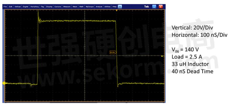
Figure 3:Switching waveform 140 VIN, 28 VOUT, 2.5 A
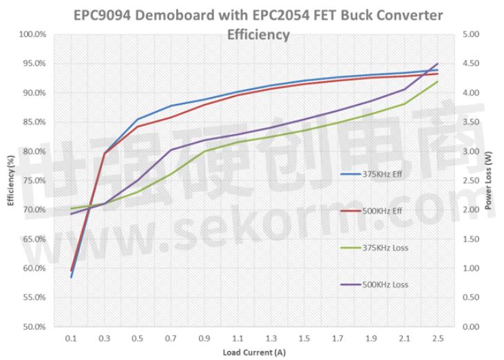
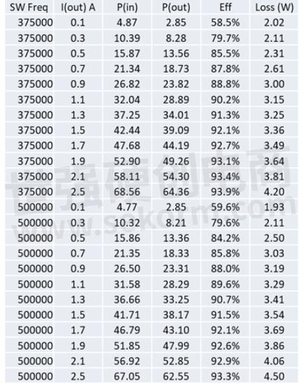
Figure 4: Efficiency and loss graph and table at 375kHz and 500kHz
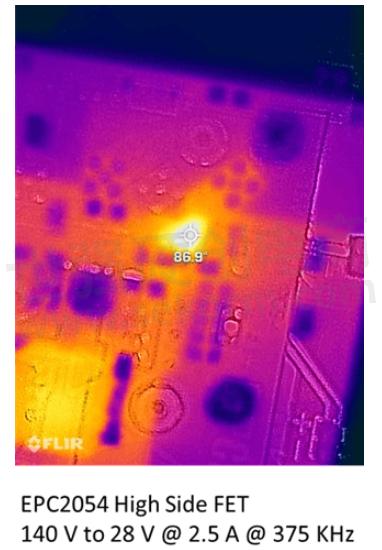
Figure 5: Thermal image of High Side FET
This article have shown that an EPC development board can easily be utilized to evaluate the performance of a given GaN FET or IC in common applications with very little setup effort. Configured the standard EPC9094 development board into a buck converter operating from 140VIN to 28VOUT at 2.5A to evaluate the performance of the 200V EPC2054 eGaN FET at various switching frequencies. With a set dead time of 40ns to allow full ZVS from high to low, the converter was able to demonstrate 94% efficiency at full power while switching at 375kHz.
- +1 Like
- Add to Favorites
Recommend
- Sharge Selects GaN FETs EPC2218 from EPC for High-power USB PD Charger Retro 67 to Achieve the Most Efficient Power Conversion
- Sekorm Became an Authorized Distributor of EPC(Efficient Power Conversion), Which Brings GaN FET Products
- 65A ePower™ Chipset from Efficient Power Conversion (EPC) Redefines Power Conversion
- EPC Introduces EPC9157 48V to 12V Demo Board Featuring EPC eGaN FETs and New Renesas DC-DC Controller
- Efficient Power Conversion (EPC) Expands 100 V eGaN FET Family Offering Designers Best-in-Class Performance and Cost for 48 V DC-DC Conversion
- GaN Power Components Will Be Cheaper Than Silicon Ones, Says EPC
- EPC‘s New EPC9165 Bidirectional Converter that Delivers 2kW with 96.8% Peak Efficiency
- GaN Transistors from EPC Bring Newest Rad Hard Technology to Demanding Space Applications
This document is provided by Sekorm Platform for VIP exclusive service. The copyright is owned by Sekorm. Without authorization, any medias, websites or individual are not allowed to reprint. When authorizing the reprint, the link of www.sekorm.com must be indicated.
Integrated Circuits


Discrete Components


Connectors & Structural Components


Assembly UnitModules & Accessories


Power Supplies & Power Modules


Electronic Materials


Instrumentation & Test Kit


Electrical Tools & Materials


Mechatronics


Processing & Customization


