4 Key Factors on Copper Plating

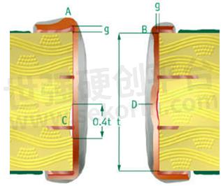
Copper plating is an essential process for PCB manufacture and has a very important influence on PCB quality. The copper inside holes connects traces between different layers and the pins of THT components. In the very beginning, the PCB boards were mainly single-layer boards, which do not have copper side holes. Nowadays, the PCBs are becoming more and more dense with higher and higher layers, and smaller and smaller vias, with the development of copper plating technology.

SDY Electronic attaches great importance to the copper plating process and has built a well-organized system to manage the copper plating process.

There are four key factors in the copper plating process to ensure good quality of copper inside holes.
(1)Board abrasion.
There are sharp edges around holes after the drilling process. So those sharp edges have to be removed by abrasion.
(2)Board cleaning.
There are dust or impurity substances attached to the holes after the drilling process and movement, which have to be cleaned completely. Otherwise, the impurity substances may cause copper to be peeled off. SDY has a super high-pressure water cleaning machine to clean the boards before copper plating. The machine integrates board abrasion function as well, so the abraded materials are washed away by water immediately.
(3)Desmear.
Part of the resin of CCL is melted due to high temperature during the drilling process, and the melted resin is distributed irregularly inside the holes. This makes the surface of the hole wall in a rough condition. It has to make the surface of holes smooth and flat, in order to plate even copper with enough and average thickness.
(4)The copper plating facility.
Automatic copper plating lines are widely used nowadays. SDY has an automatic copper plating line, integrating desmear process with automatically controlled specifications. This not only increases the copper plating efficiency but also ensures the quality of copper plating.
Please feel free to contact SDY for any further questions or remove your worries about the copper plating of your PCB projects.
- +1 Like
- Add to Favorites
Recommend
- SanDeYing Electronic PCB 3D Models Provides A Clear View of All The Parts on PCB Boards in 3 Dimensions Length, Width, and Height
- Selection of Fuses in Small Home Appliance PCB Board
- Four Points to Control the PCB Cost: PCB Layers, PCB Dimensions, Manufacturing Difficulty and PCB Sheet Material
- Waermtimo High-Strength Thermal Pads Help PCB Conduct Heat Effectively
- The Role of Thermal Gel and the Heat Dissipation Application of PCB Board
- What Is the Design Standard of PCB Pad?
- PCB Adapters: Time-saving Termination Designed for Printed Circuit Boards with Thickness up to 2.4 mm
- What is the HDI (High-Density Interconnect) Printed Circuit Boards?
This document is provided by Sekorm Platform for VIP exclusive service. The copyright is owned by Sekorm. Without authorization, any medias, websites or individual are not allowed to reprint. When authorizing the reprint, the link of www.sekorm.com must be indicated.


