A Brief History of Power Transistors for Engineers

In this article, we reflect on the history of semiconductors from the early days of Bipolar Transistors to the present advancements and promise of gallium nitride (GaN) FETs and ICs.
Overview of Semiconductors and Their Uses
Semiconductors play a crucial role in the modern world of electronics. Semiconductors are materials that have electrical conductivity between that of a conductor (such as copper or aluminum) and an insulator (such as rubber or glass). Some common semiconductors include silicon, silicon carbide, and gallium nitride.
Semiconductors include components such as transistors, diodes, and integrated circuits. Transistors are the basic building blocks of most modern electronic devices, including computers, smartphones, and televisions.
The Early History of Semiconductors: Pre-20th Century
The history of semiconductors dates to the late 19th century when scientists first began to study the electrical properties of materials. One of the key discoveries of this era was the observation that some materials could produce an electric current when exposed to light. This phenomenon was later called the photoelectric effect and paved the way for the development of solar cells.
Early semiconductors presented several challenges that needed to be overcome to develop practical and reliable semiconductor devices. Some of the main challenges included:
Material purity: To function properly, semiconductor materials must be extremely pure, with impurities measured in parts per billion. Achieving this level of purity was a major technical challenge in the early days of semiconductor development.
Fabrication techniques: The development of reliable techniques for fabricating semiconductor devices, such as doping and photolithography, was also a major challenge, as these techniques required precise control of materials and processes and the development of specialized equipment and manufacturing processes.
Heat dissipation: As semiconductor devices became more complex and powerful, they generated more heat, which could damage the device and affect its performance.
Size limitations: Early semiconductor devices were relatively large, which limited their practical applications. Developing techniques for creating smaller and more densely packed devices, such as integrated circuits, was a major breakthrough in semiconductor technology.
Overcoming these challenges required significant advances in materials science, manufacturing processes, and engineering.
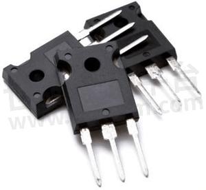
The Development of the Bipolar Transistor
The predecessor to the ubiquitous modern-day transistor was the bipolar transistor. The bipolar transistor is a type of transistor that uses both electrons and holes to carry current. The bipolar transistor quickly replaced vacuum tubes as the primary component in electronic circuits, due to its smaller size, greater efficiency, and lower power consumption. It enabled the development of a wide range of electronic devices, such as radios, televisions, and computers, and paved the way for the development of more advanced semiconductor technologies, such as the integrated circuit.
Although the bipolar transistor represented a significant breakthrough in semiconductor technology, it also presented several challenges that needed to be overcome. Bipolar transistors are made of multiple layers of semiconductor material, which requires complex manufacturing processes and precise control of materials and processes. This made them difficult and expensive to produce in large quantities. Bipolar transistors are also relatively inefficient compared to other types of transistors, meaning they consume more power and generate more heat. Early bipolar transistors were relatively large which limited their practical applications, and they were prone to generating electrical noise, which can interfere with the proper functioning of electronic circuits.
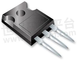
Evolving to the Silicon power MOSFET
The evolution from the bipolar transistor to the silicon power MOSFET (Metal-Oxide-Semiconductor Field-Effect Transistor) began in the 1960s when engineers started to investigate alternative transistor designs that could address some of the challenges presented by bipolar transistors.
One of the main advantages of the MOSFET is its low power consumption, which makes it more efficient than bipolar transistors. MOSFETs are also relatively simple to manufacture and can be produced in large quantities at low cost. In the 1970s, engineers began to develop MOSFETs that were optimized for power applications, known as power MOSFETs. These devices were designed to handle high voltage and high current levels and were able to switch on and off rapidly, making them suitable for use in power electronics applications such as motor drives, power supplies, and inverters. Today, power MOSFETs are widely used in a range of power electronics applications, from consumer electronics to industrial and automotive systems.
As with the bipolar transistor, silicon power MOSFETs have reached the end of the road in delivering better performance at a consistently declining cost. Fortunately, the quest for the ideal switch that has infinitely fast switching speed, no electrical resistance, and a lower cost has not slowed, and new base semiconductor materials upon which to build high-performance power conversion transistors and integrated circuits have emerged.
The Recent History of Power Transistors to Present Day
The evolution from silicon power MOSFETs to gallium nitride (GaN) FETs began in the 1990s when researchers started to explore the potential of GaN as a semiconductor material for power electronics. GaN is a wide-bandgap material that offers several advantages over traditional semiconductor materials such as silicon, including higher breakdown voltages, higher operating temperatures, and faster switching speeds.
In the early 2000s, researchers developed the first GaN-based power transistors, which were initially used in niche applications. However, as the manufacturing processes for GaN transistors became more refined, their cost decreased, and their performance improved. This led to the development of GaN FETs that were optimized for power electronics applications.
How Gallium Nitride Solves Challenges of the Past
One of the main advantages of GaN FETs is their ability to switch on and off at much higher frequencies than silicon power MOSFETs, which enables the development of more efficient power electronics systems. GaN FETs also have lower switching losses than silicon power MOSFETs, which reduces the amount of heat generated during operation and improves overall efficiency. Another advantage of GaN FETs is their ability to handle high voltages, which makes them suitable for use in a range of high-power applications such as electric vehicles, renewable energy systems, and data centers.
The Future of Semiconductor Technology with Gallium Nitride at its Core
The future of semiconductors is promising, with ongoing research and development efforts focused on improving the performance, reliability, and cost-effectiveness of advanced semiconductor devices. Wide-bandgap semiconductors such as GaN, are paving the way for a range of new applications and technologies. The advantages that GaN offers can lead to significant improvements in efficiency and reduce energy waste in many applications. As GaN technology continues to mature it is expected to lead to significant cost reductions and continued improvements in device performance and reliability.
Find Your GaN Power Solution
After this brief history of semiconductors, we invite you to continue the quest for the ideal switch by exploring our family of GaN FETs and ICs. For design assistance try the growing array of design tools, models, and performance simulations in the GaN Power Bench or contact us directly.
- +1 Like
- Add to Favorites
Recommend
This document is provided by Sekorm Platform for VIP exclusive service. The copyright is owned by Sekorm. Without authorization, any medias, websites or individual are not allowed to reprint. When authorizing the reprint, the link of www.sekorm.com must be indicated.
Integrated Circuits


Discrete Components


Connectors & Structural Components


Assembly UnitModules & Accessories


Power Supplies & Power Modules


Electronic Materials


Instrumentation & Test Kit


Electrical Tools & Materials


Mechatronics


Processing & Customization


