What Is Ion Implantation Of Silicon Carbide?

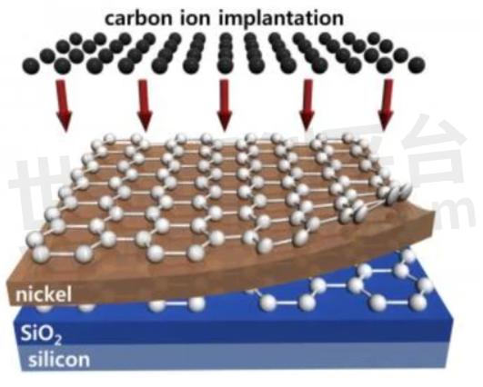
Ion implantation of silicon carbide is a technique used to introduce specific impurity atoms in silicon carbide materials. Ion implantation typically implants desired dopants into silicon carbide crystals by means of a high-energy ion beam.
The ion implantation process includes the following steps:
1. Select the target impurity atoms to be implanted, usually boron (B), nitrogen (N) or phosphorus (P), etc.
2. Prepare the SiC substrate and film to support and protect the ion implantation process.
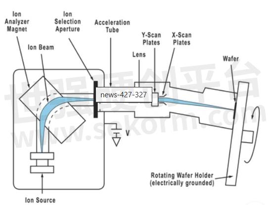
3. Use an ion implanter to introduce a high-energy ion beam into the silicon carbide material. A beam of ions passes through the membrane and is implanted into the silicon carbide crystal.
4. After the implantation is completed, other process steps such as annealing, cleaning, and electrode formation are used to convert the ion-implanted material into a functional device.
Selective doping technology is a method of controlling the ion implantation process.It uses photolithography and film technology to precisely define and control the ion implantation area during the manufacturing process. Masks are created in targeted areas by applying photoresist to specific areas and performing steps such as exposure and development. This mask prevents ions from entering the material from the protected areas, enabling selective doping. Selective doping techniques can be used to create specific doped regions in silicon carbide materials, thereby optimizing the material's electronic properties and device performance.
All in all, the ion implantation of silicon carbide is a technology that introduces specific impurity atoms into the material, and selective doping technology is a method of controlling the ion implantation process. Doping is achieved in a specific area through mask technology to achieve Optimizing the performance of silicon carbide materials.
- +1 Like
- Add to Favorites
Recommend
- Silicon Labs Expands Isolated Gate Driver Product Family Ideal for Hybrid and Electric Vehicles (EV)
- Silicon Labs Simplifies IoT Development with Simplicity Studio 5
- Silicon Labs Z-Wave Wireless Selected for Johnson Controls Next Generation Qolsys Smart Home Panel
- Silicon Labs Strengthens Isolated Gate Driver Portfolio
- News | Silicon Labs and Amazon Collaborate on Sidewalk, a New Shared Network for IoT Consumer Devices
- Software Speeds Development of IEEE 1588 System Integration | Silicon Labs
- Silicon Labs and Skyworks reach agreement to sell infrastructure and automotive business
- A 12V DC Lightning Protection Solution from Yint
This document is provided by Sekorm Platform for VIP exclusive service. The copyright is owned by Sekorm. Without authorization, any medias, websites or individual are not allowed to reprint. When authorizing the reprint, the link of www.sekorm.com must be indicated.
Integrated Circuits


Discrete Components


Connectors & Structural Components


Assembly UnitModules & Accessories


Power Supplies & Power Modules


Electronic Materials


Instrumentation & Test Kit


Electrical Tools & Materials


Mechatronics


Processing & Customization


