3PEAK Releases High-PSRR, High-Bandwidth and High-Voltage Operational Amplifiers TPA267x

The semiconductor supplier 3PEAK (stock code: 688536), which focuses on high-performance analog devices and embedded processors, has officially released the TPA267x series of high-PSRR, high-bandwidth, and high-voltage Operational Amplifiers.
The TPA267x series products have a bandwidth of 10 MHz, a slew rate of 15 V/µs, and a rejection ratio of 80 dB under a 100-kHz power supply interference, reducing the design cost of customers on the power supply. The products are widely used in industrial automation, photovoltaic energy storage, motor drives, and audio equipment.
Features of TPA267x
Power supply voltage: 4 V – 36 V
Quiescent current: 1.65 mA
Offset voltage: ±3 mV
Offset voltage temperature drift: 2 μV/℃
High bandwidth: 10 MHz
High slew rate: 15 V/μs
High PSRR+: 80 dB@100 kHz
Operating temperature range: −40℃ to 125℃
Advantages of TPA267x
TPA267x has excellent power supply rejection ratio (PSRR+) characteristics in the full voltage supply range, ensuring the consistency and stability of performance, and is very suitable for applications in various industrial power supply environments. In addition, the offset voltage temperature drift of TPA267x is only 2 μV/℃, ensuring accurate signal sampling in the full temperature range. Its typical application circuit is shown in the figure below.
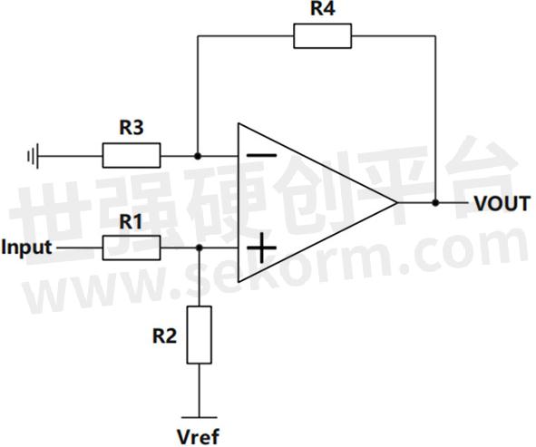
Typical Application Circuit of TPA267x
In the above application circuit, the key characteristics of the amplifier are crucial to the entire signal acquisition system, mainly reflected in the following aspects:
1. High PSRR characteristics in the full supply voltage range
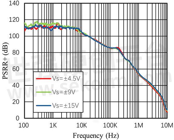
The power supply rejection ratio (PSRR+) is a key indicator that affects the output accuracy of the amplifier. It is defined as the ratio of the change in the power supply voltage (ΔVs) to the change in the amplifier offset voltage (ΔVos), usually in dB. The change in the offset voltage will be amplified by the noise gain of the amplifier circuit, thereby affecting the output accuracy. The definition of PSRR is as follows:
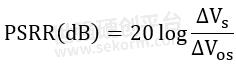
In most application scenarios, high-frequency noise is often superimposed on the power supply, and this noise is coupled to the supply pins of the amplifier through the power supply path. The high-frequency PSRR capability of the amplifier can effectively suppress the influence of the noise on the accuracy of the output signal. As shown in the figure below, TPA267x exhibits excellent high-PSRR+ performance, with PSRR+ exceeding 80 dB, that is, 100 μV/V at a frequency of 100 kHz. This high-performance PSRR+ characteristic allows TPA267x to maintain high signal accuracy in a high-frequency noise environment.
TPA267x PSRR+ and Frequency
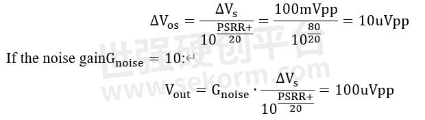
When a 100-kHz frequency is coupled to the power supply, and the peak-to-peak value is 100 mVpp high-frequency noise, the change in the input offset voltage caused by the power supply noise is 10 uVpp:
The TPA267x series maintains highly consistent PSRR+ performance in all power supply voltage ranges, whether under low or high voltage supply conditions, without fluctuating with power supply changes, meeting the adaptation requirements of customers for different power supply conditions.
2. The static power consumption current is significantly reduced
TPA267x has further optimized the quiescent current. Under typical operating conditions at 25℃, the quiescent current of a single channel is 1.65 mA (typical value). The maximum quiescent current does not exceed 2.5 mA over the full temperature range. Compared with the previous generation of high-voltage High-Bandwidth Operational Amplifiers, TPA267x achieves a reduction of 45% and 37.5% in quiescent current, respectively. Under the same ambient temperature, the heat generated by the device is significantly reduced, and it has a wider operating temperature range, thereby providing excellent energy consumption performance. As shown in the figure below, the quiescent current fluctuates minimally within the operating temperature range of –40℃ to 125℃. Therefore, in application environments with large external temperature changes, TPA267x can also maintain a stable quiescent current.
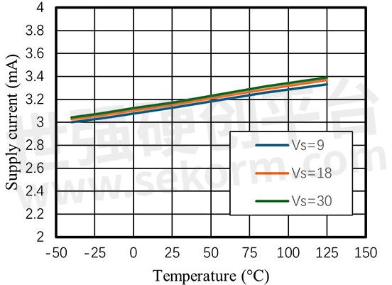
TPA2672 Supply Current and Temperature
3. Low offset voltage temperature drift ensures sampling accuracy over the entire temperature range
The TPA267x series not only has a low input offset voltage, with a maximum of only ±3 mV (Ta = 25℃), but also has an input offset voltage temperature drift of only 2μV/℃ (typical value). This characteristic is crucial for applications sensitive to input offset voltage, such as current sensing applications that require high closed-loop gain. The low offset voltage temperature drift ensures that the input offset voltage changes minimally over the entire temperature range, which not only ensures that the detection circuit can maintain high accuracy over the entire temperature range but also significantly reduces the sampling calibration cost for customers. As shown in the figure below, due to its excellent offset voltage temperature drift performance, the input offset voltage of TPA267x is very insensitive to temperature changes, making it an ideal choice for sensitive applications.
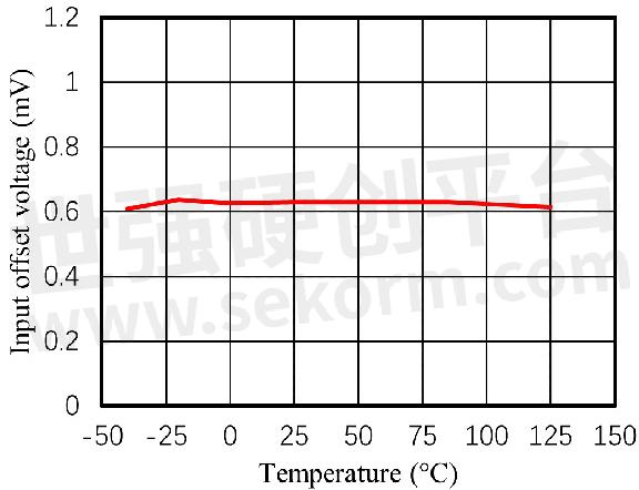
TPA267x Input Offset Voltage and Temperature
4. No glitches in the output signal during the power-up and power-down transitions
Some amplifiers may generate short pulses in the output signal during the power-up or power-down transition when the supply voltage is below the minimum operating voltage. This is because of the instability of internal circuit nodes, and the amplitude and width of these short pulses are usually related to the power-up and power-down speed and amplitude of the power supply. If the subsequent system is sensitive to such short pulses, it may cause malfunctions. For example, in applications such as overcurrent protection or overvoltage protection, short pulses during power-up may cause false triggering of the protection mechanism, thereby adding additional costs to the user. To solve this problem, the TPA267x series has been optimized in design. As shown in the figure below, it ensures that the output signal does not generate false pulses during the power-up and power-down transitions.
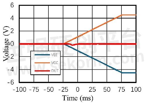
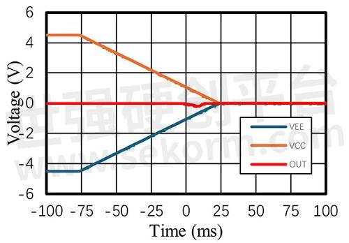
Power-up and Power-down of TPA267x
TPA267x is now in mass production. Sample and evaluation board services are also available.
- +1 Like
- Add to Favorites
Recommend
- 3PEAK‘s Automotive-Grade Test Center Officially Commences Operations
- 3PEAK Showcases Multiple Auto-grade Products at Auto China 2024
- 3PEAK Isolation Products Are Certified to a Full Range of Safety Standards Including VDE, TÜV, UL, CSA, CQC, and CB
- The Only Company in China Included in the IBEE ESD Report! 3PEAK‘s Complete Series of Automotive CAN Transceivers in Mass Production
- 3PEAK Achieves ISO 26262:2018 ASIL D Process Certification, the Highest Level of Automotive Functional Safety
- 3PEAK Unveiled a Next-Generation Automotive-grade High-current Linear Regulator TPL8151Q Supporting Wide Range Input of 29V
- 3PEAK Unveiled Automotive High-Voltage, Low-quiescent Current Voltage Monitor TPV8368Q with High Sense Voltage up to 36V
- 3PEAK Becomes the First Chip Maker in China to Have Two Types of CAN Transceivers Passed German C&S Compatibility Certification at the Same Time
This document is provided by Sekorm Platform for VIP exclusive service. The copyright is owned by Sekorm. Without authorization, any medias, websites or individual are not allowed to reprint. When authorizing the reprint, the link of www.sekorm.com must be indicated.
Integrated Circuits


Discrete Components


Connectors & Structural Components


Assembly UnitModules & Accessories


Power Supplies & Power Modules


Electronic Materials


Instrumentation & Test Kit


Electrical Tools & Materials


Mechatronics


Processing & Customization


