XBLW LM239 Precision Voltage Comparator Chip with 0.2mA Extremely Low Power Supply Current, Can Be Powered by A Single Power Supply over A Wide Voltage Range

New Product Introduction
XBLW LM239 Precision voltage comparator chip
1、Product Overview
This series of devices consists of four independent precision voltage comparators, and the offset voltage of LM239DTR is as low as 5mV. Each comparator is specially designed to be powered by a single power supply over a wide voltage range. Separate power sources can also be used for operation.
2、Chip Features
● Single power supply voltage range or dual power supply:+2 to+36 V or ± 1 V to ± 18 V
● Extremely low power supply current (0.2 mA), independent of power supply voltage
● Low input bias current: 25 nA (typical value)
● Low input offset current: ± 5 nA (typical value)
● Low input offset voltage: ± 2 mV (typical value)
● The input common mode voltage range includes ground voltage
● Low output saturation voltage: 250 mV (typical value); (ISINK=4mA)
● The differential input voltage range is equal to the power supply voltage
● TTL, DTL, ECL, MOS, CMOS compatible outputs
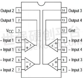
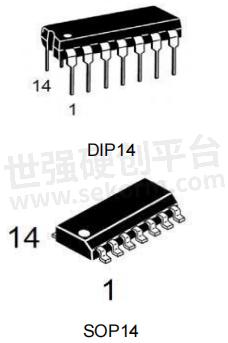
3、Pin Definition and Packaging Type


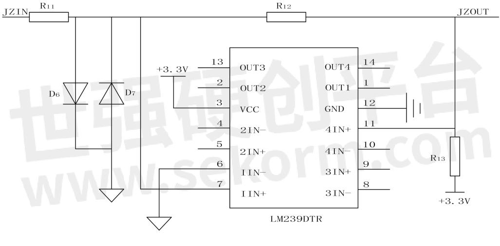
4、 Introduction and Application Principles of Typical Application Circuits

The LM239DTR application circuit - radar cone scan reference signal acquisition circuit uses the voltage comparator chip XBLW LM239DTR, and uses diodes to limit and shape the input cone scan reference signal. The 3.3V of the circuit is a square wave signal, The period is the same as the input signal, and the rising edge of the square wave is considered as the reference signal for cone scanning Phase zero point.
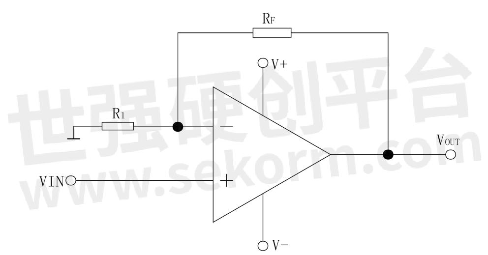
Application Principle: What is A Voltage Comparator?
Simply put, a voltage comparator compares the magnitude of two analog voltages (or two digital voltages, which are not described here) and determines which voltage is higher, as shown in Figure 1. Figure 1 (a) shows a comparator with two input terminals: the in-phase input terminal ("+" terminal) and the in-phase input terminal ("-" terminal), and an output terminal Vout (output level signal). In addition, there is a power supply V+and ground (this is a single power comparator), with the same phase input voltage VA and the opposite phase input VB. The changes in VA and VB are shown in Figure 1 (b). From time 0 to t1, VA>VB; from t1 to t2, VB>VA; from t2 to t3, VA>VB. In this case, the output of Vout is shown in Figure 1 (c): When VA>VB, Vout outputs a high level (saturated output); When VB>VA, Vout outputs a low level. You can determine which voltage is higher based on the output level.

5、Chip Application
● Alarm circuit
● Automatic control circuit
● Power supply voltage monitoring circuit
● Oscillators and voltage controlled oscillators circuits
- +1 Like
- Add to Favorites
Recommend
- XBLW Showcased Linear Voltage Regulator XBLW AMS1117, RS-485/RS-422 Chip MAX3485 and Other Product in 2023 ES SHOW
- Application Of XBLW Products On Fascia Guns
- Xinbole (XBLW) Attended the Shanghai Munich Electronics Show, July 8-10, 2024
- XBLW LM2576S Series Is A New 3A Current Output Buck Switch Regulated Integrated Circuit
- Real-Time Clock (RTC) Chips XBLW DS1302 & DS1307: Powerful And Reliable
- 20V 5A DC Bidirectional Motor Driver Circuit Chip - XBLW CP2119, with A Working Voltage Range of 3V to 20V, Compatible for SS6285L
- Programmable Resolution Single-Bus Temperature Sensor - XBLW DS18B20 Offers Temperature Measurement With A Resolution of 9 To 12 Bits
- About XBLW MC34063 DC-DC Converter Control Circuit Test Share
This document is provided by Sekorm Platform for VIP exclusive service. The copyright is owned by Sekorm. Without authorization, any medias, websites or individual are not allowed to reprint. When authorizing the reprint, the link of www.sekorm.com must be indicated.


