About XBLW MC34063 DC-DC Converter Control Circuit Test Share

The article chapter before the speech
At present, DC/DC converters are widely used in remote and data communication, computers, office automation equipment, industrial instrumentation, energy storage, audio-visual multimedia and other fields, involving all walks of life in the national economy. Taking XBLW MC34063 circuit as an example, this paper introduces its electrical characteristics and the test method of its booster circuit, analyzes its test principle and the points for attention in the design of booster circuit, and provides some reference for the analysis and production test of DC/DC converters by the majority of users.
一、Quotation
XBLW MC34063 integrated circuit itself contains the main functions required by DC/DC converter, is a bipolar linear integrated monolithic control circuit, due to cost-effective, switching peak current up to 1.5a, the circuit is simple and the efficiency meets the general requirements. therefore, it is widely used in microprocessor (MPU) or MCU based systems. This paper takes our XBLW MC34063 integrated circuit as an example to discuss the test method of dc/dc conversion circuit.
二、The circuit interface is shao
XBLW MC34063 circuit introduction
The XBLW MC34063 circuit is composed of a reference voltage generator with automatic temperature compensation function, a comparator, a duty cycle controlled oscillator, an R-S Flip-Flop and a high-current output switching circuit. The device can be used as the control core of boost converter, buck converter and reverse converter, and the DC/DC converter composed of it is simple and reliable, and only uses a few external components.
Main features: input voltage range of 2.5~40V, output voltage adjustable range of 1.25~40V, output current up to 1.5A, operating frequency up to 180kHz, low static current, short circuit current limit, can achieve boost or buck power converter.
The basic structure and pin function are shown in figure 1:
Pin1: switch tube T1 collector outlet;
Pin2: T1 emitter outlet of the switch tube;
Pin3: timing capacitor CT terminal, adjusting CT can make the operating frequency change in the range of 100~100 KHz;
Pin4: power source;
Pin5: the inverting input end of the voltage comparator is also the output voltage sampling end, which should be connected with two precision resistors with an accuracy of not less than 1% when used;
Pin6: power end;
Pin7: peak load current (Ipk) sampling terminal; 6, 7 when the voltage between the pins exceeds 300mV, the chip will start the internal overcurrent protection function;
Pin8: drive tube T2 collector outlet.
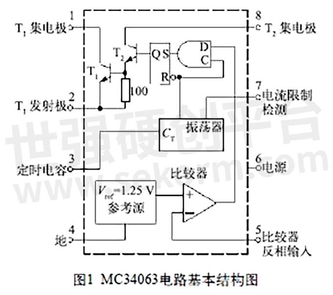
Working principle: the oscillator is continuously charged and discharged by a timing capacitor connected to the CT Pin (Pin 3) from a constant current source to generate an oscillating waveform. Both charge and discharge currents are constant, so the oscillation frequency depends only on the capacity of the external timing capacitor. The C input of the gate is high when the oscillator is charged externally; D the input side is high when the input level of the comparator is below the threshold. When both inputs C and d become high level, the trigger is set to high level and the output switch tube is on. Conversely, when the oscillator is discharging, the C input is low and the flip-flop is reset, leaving the output switch tube in the off state. The current limit detection terminal Pin7 performs its function by detecting the voltage drop on the resistor connected between the VCC and Pin7. When the voltage drop across the resistor is detected to approach more than 300 mV, the current limiting circuit begins to work. At this time, the timing capacitor is quickly charged through the CT Pin (Pin3) to reduce the charging time and the on-time of the output switch tube, resulting in a longer closing time of the output switch tube.
三、Circuit performance electrical parameter test description
XBLW MC34063 circuit performance electrical parameter test description
The test of the circuit includes the oscillator part, the output switch part, the comparator part, the whole device, and the application part such as voltage boost. The following is a description of the main parameters of each part of the test method.
1、Qscillator section
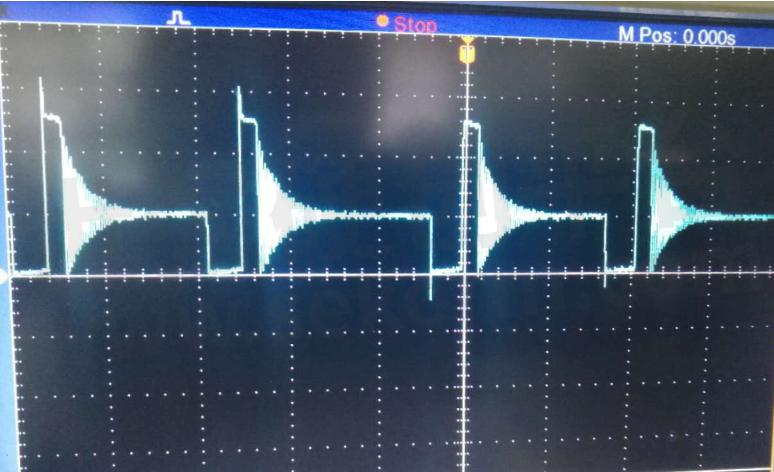
Some parameters of the oscillator are tested, including oscillator frequency (Fosc), charge current (Ichg), discharge current (Idischg), discharge charge current ratio (Idischg/Ichg), current limit detection voltage (Vipk). When the voltage is applied according to the test conditions, the input timing capacitor will produce the charge-discharge triangle waveform as shown in figure 2, according to which the oscillator frequency can be known. According to the formula I=C×ΔV/Δt, its charge-discharge current can be calculated, and VCC= VPin7 = 5V. As shown in figure 2, the charging process of the timing capacitor is significantly greater than the discharge process. Until the current limiting circuit starts to work, the timing capacitor is quickly charged through the CT Pin (Pin3) to reduce the charging time and the on-time of the output switch tube. As a result, the discharge time and the closing time of the output switch tube are extended. When the charging time and the discharge time are equal, the pressure difference between VCC And Vpin7 is the current limiting detection voltage Vipk.
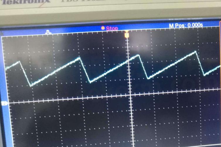
图2 三角波充放电波形图
According to the charge-discharge triangle waveform in figure 2, the oscillator frequency can be known according to the formula I=C×ΔV/Δt, the charge-discharge current can be calculated, and VCC=Vpin7= 5V. From figure 2, it can be seen that the timing capacitor charging process is significantly greater than the discharge process, and the vpin7 voltage is adjusted downward until the current limiting circuit starts to work. At this time, the timing capacitor is quickly charged through the CT Pin (Pin3) to reduce the charging time and the on-time of the output switch tube, resulting in the discharge time and the closing time of the output switch tube being extended. When the charging time and discharge time are equal, the pressure difference between VCC And Vpin7 is the current limiting detection voltage Vipk.
2、Output switch section
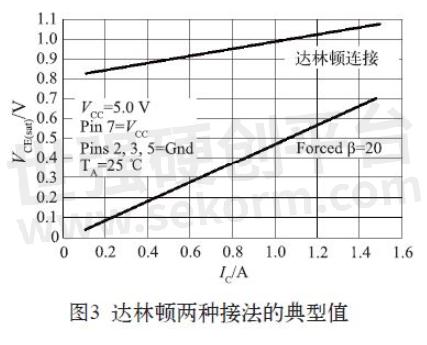
In order to meet the requirements of 1.5A peak switching current, darlington connection is usually used. the output from Pin5 to the CE poles of the t1 tube involves the oscillator, gate, and R-S flip-flop. If the t1 tube is to be on, the oscillator output signal must be maintained in the logical 1 state. Figure 3 shows the typical values of the two darlington connections.
3、Comparator section
When the input voltage of Pin5 is lower than the internal Vref, Pin2 will output a square wave of 24-42 KHz, VOL=0 V, and VOH is VCC/2. When the input voltage of Pin5 is higher than the internal Vref, the output of Pin2 is 0 V. Thus, the Vref value is Vth. This test is completed together with the oscillator charge and discharge frequency. Vth electrical parameter table specification is 1.21~ 1.29V (operating temperature is 0~70 ℃), mass production test is usually normal temperature, taking into account the error in the test, the specification can be set to 1.225~ 1.275V range.
四、Test and research on building booster circuit
Test and research on building a boost circuit with XBLW MC34063
DC/DC converters are voltage converters that effectively output a fixed voltage after converting the input voltage. They are generally divided into three categories: boost DC/DC converters, buck DC/DC converters, and reverse DC/DC converters. the following is the test method of the booster circuit composed of XBLW MC34063. Test and research on building a boost circuit with XBLW MC34063
DC/DC converters are voltage converters that effectively output a fixed voltage after converting the input voltage. They are generally divided into three categories: boost DC/DC converters, buck DC/DC converters, and reverse DC/DC converters. The following is the test method of the booster circuit composed of XBLW MC34063.
1、Principle of booster circuit
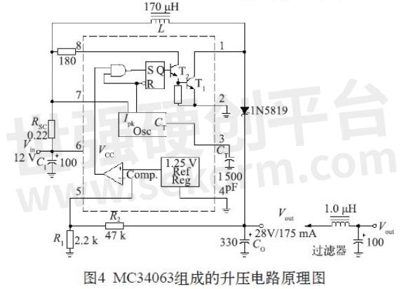
The principle of the boost circuit composed of XBLW MC34063 is shown in figure 4. When the switch tube T1 in the chip is switched on, the input voltage vin is grounded by the sampling resistance RSC, inductor L, Pin1 and Pin2. At this time, the inductor L begins to store energy, while CO provides energy to the load. When T1 is disconnected, the input voltage vin and the inductor L provide energy to the output load and the capacitor CO simultaneously through the diode 1N5819. During the release of energy, the electromotive force polarity at both ends of the inductor L is the same as the polarity of the input voltage vin, which is equivalent to two power supplies in series, and CO stores the current from the inductor L. After several switching cycles (Figure 5), the voltage of the output capacitor co rises, resulting in the output voltage Vout being higher than the input voltage Vin. The frequency at which the switching tube is on and off is also the operating frequency of the OSC part of the oscillator. As long as this frequency is high enough in relation to the time constant of the output load, a continuous dc voltage can be obtained on the output load. The output voltage is divided by the voltage divider R1 and R2 and then input to the comparator, and the pulse width is controlled together with the reference voltage to obtain the required voltage, namely Vout=Vref× (R1/R2+1).
2、Test methods and results
The test parameters of the booster circuit are shown in table 1. The linear adjustment rate is the relative change of the output voltage vout caused when the input voltage vin changes from 8 V to 16 V under specified conditions. Load adjustment rate is the relative change of output voltage vout when the output current IO changes from 75 MA to 175 MA under specified conditions. The output ripple is to adjust the size of the output load under the specified conditions, so that the output current IO=175 MA, read the ac component peak - peak value contained in the output voltage Vout with the oscilloscope, pay attention to the influence of external interference on the ripple measurement, can make the ground line between the oscilloscope ground terminal and the XBLW MC34063 ground terminal as short as possible. Generally not more than 10 cm, or the equivalent method of external circuit compensation; efficiency is the percentage of output power to input power.
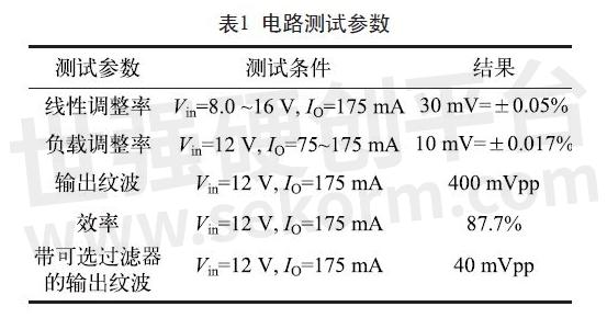
The booster circuit is not connected with a high-power darlington structure switch tube, which is mainly used in the occasions where the output current is small, and the working current can reach tens to hundreds of ma. The test results show that the output stability is high and the conversion efficiency can reach more than 88%.
3、Considerations for designing MC34063 circuits
The design of this test circuit requires special attention (see figure 4) : first, on the PCB board layout, CI and CO should be as close as possible to the circuit under test, which can reduce the copper trace resistance that affects the Vin and Vout ripple. Minimizing the trace length between the inductor l and the output diode 1N5819 can reduce power consumption and improve efficiency. The distance between the output feedback resistor R2 and the inductor L minimizes noise effects. Secondly, in the selection of capacitance, since the input of the booster circuit is a triangular voltage waveform, the input capacitance CI must reduce the input ripple and noise. The size of the ripple is inversely proportional to the size of the input capacitance value, and the larger the capacitance value, the smaller the ripple. If the output load changes very little and the output current is small, it is also safe to use a small capacity input capacitor. If the input voltage of the circuit under test differs very little from the source output, a small volume capacitor can also be selected. If the circuit is required to interfere very little with the ripple of the input voltage source, large capacity capacitors may be required and/or the equivalent series resistance is reduced. The choice of output capacitance CO is determined by the output voltage ripple. In most cases, use capacitors with low equivalent series resistance, such as ceramic and polymer electrolytic capacitors. Otherwise, it is necessary to carefully look at the frequency compensation of the circuit under test, and an additional capacitor may be required at the output circuit end. Third, because the size of the inductance L affects the input and output ripple voltage and current, the choice of inductance is also the key to the design. The conversion efficiency of inductors with low equivalent series resistance is the best. The inductance saturation current rating should be greater than the steady-state peak inductance current of the circuit. Finally, choose a fast schottky rectifier diode (e.g. 1N5819). Compared with ordinary diodes, schottky diodes have low power consumption and high switching frequency. The schottky diode average voltage rating should be greater than the maximum output voltage of the circuit.
五、General knot
The above is from the perspective of the structure and working principle of XBLW MC34063 integrated circuit, the basic electrical parameters and the test method of its booster circuit are explained, which provides a certain reference for the peer test of this type of DC/DC circuit.
- +1 Like
- Add to Favorites
Recommend
This document is provided by Sekorm Platform for VIP exclusive service. The copyright is owned by Sekorm. Without authorization, any medias, websites or individual are not allowed to reprint. When authorizing the reprint, the link of www.sekorm.com must be indicated.


