Analysis of the Production Process and Characteristics of ZMM3V3 Voltage Regulator Diode

Voltage Regulator Diodes, also known as Zener diodes or reverse breakdown diodes, are a special type of silicon diode designed to stabilize voltage in circuits. Among the various models of voltage regulator diodes, the ZMM3V3 stands out for its precise voltage regulation (3.3V), moderate power rating (500mW), and extremely low reverse current (2μA@1V), making it widely used in various electronic devices. This article will delve into the production process and characteristics of the ZMM3V3 voltage regulator diode.
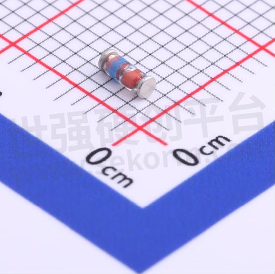
SLKOR Voltage Regulator Diode ZMM3V3 product photo
Overview of ZMM3V3 Voltage Regulator Diode
The ZMM3V3 voltage regulator diode is a semiconductor device with precise voltage regulation capabilities. With a nominal voltage of 3.3V, it can maintain a stable output voltage of 3.3V under normal operating conditions. Additionally, its power rating of 500mW meets the power requirements of most electronic devices. Noteworthy is its extremely low reverse current of 2μA@1V, providing excellent performance in standby or low-power modes.
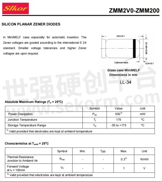
Slkor Voltage Regulator Diode ZMM3V3 specification
Analysis of the Characteristics of ZMM3V3 Voltage Regulator Diode
Precise voltage regulation: The ZMM3V3 voltage regulator diode offers precise voltage regulation at 3.3V, ensuring voltage stability in circuits to enhance overall circuit stability and reliability.
Moderate power rating: With a power rating of 500mW, it meets the power demands of most electronic devices without excessive energy loss.
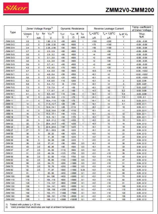
Parameters of Slkor Voltage Regulator Diode ZMM3V3
Extremely low reverse current: The ZMM3V3 boasts an ultra-low reverse current of 2μA@1V, delivering outstanding performance in standby or low-power modes. The minimal reverse current aids in reducing circuit power consumption and heat generation.
Good temperature stability: The ZMM3V3 voltage regulator diode exhibits stable performance over a wide temperature range, making it adaptable to various complex working environments.
Production Process and Analysis of Voltage Regulator Diode:
Production Process Flow
The production process of a voltage regulator diode mainly involves the following steps:
● Material preparation: This includes preparing materials such as silicon wafers, doping agents, and oxidants, where the quality and purity of these materials directly impact product performance.
● Wafer preparation: Processing silicon wafers to create individual or multiple PN junction wafers, requiring precise control to ensure PN junction quality and performance.
● Mask photolithography: Transferring mask patterns onto silicon wafers and performing processes like photoresist coating and development to form diffusion regions and doping areas, where precision affects PN junction geometry and position.
● Diffusion: Introducing doping agents into silicon wafers through high-temperature diffusion to create doping and diffusion regions, with temperature and time control crucial for product stability and reliability.
● Oxidation: Placing silicon wafers in oxidation furnaces with oxidants to form oxide layers on the surface and diode isolation layers, where thickness and uniformity affect product performance.
● Metallization: Depositing metal at the anode and cathode of the diode to create metal contacts for easy lead-out, with quality influencing product conduction capability and reliability.
● Dicing: Cutting wafers into individual voltage regulator diode chips, where accuracy affects product dimensions and appearance.
● Packaging: Packaging voltage regulator diode chips into various product forms, ensuring product safety and reliability during the packaging process.
Production Process Issues and Solutions
1. Material issues:
● Insufficient doping, uneven doping, inadequate purity, etc., may lead to unstable product performance.
● Solution: Select high-quality, high-purity raw materials and rigorously control doping agent concentration and uniformity.
2. Mask photolithography issues:
● Lack of precision in mask photolithography may result in inaccurate PN junction geometry and position.
● Solution: Employ high-precision mask photolithography equipment and techniques to ensure PN junction accuracy and position.
3. Diffusion issues:
● Improper temperature and time control during diffusion may compromise product stability and reliability.
● Solution: Strictly control diffusion process temperature and time to ensure thorough diffusion and reaction of doping agents with silicon wafers.
4. Oxidation issues:
● Inadequate thickness and uniformity of oxide layers may impact product performance.
● Solution: Optimize oxidation furnace process parameters to meet the required thickness and uniformity of oxide layers.
5. Metallization issues:
● Poor quality metallization may reduce product conduction capability and reliability.
● Solution: Use high-quality metal materials and advanced metallization techniques to ensure the quality and reliability of metal contacts.
6. Dicing and packaging issues:
● Inadequate dicing accuracy and poor packaging may result in product dimensions and appearance not meeting requirements, potentially affecting product safety and reliability.
● Solution: Utilize high-precision dicing equipment and adhere to strict packaging standards to ensure product dimensions and appearance meet requirements while guaranteeing product safety and reliability.
- +1 Like
- Add to Favorites
Recommend
- The Voltage Regulator Diode ZMM3V9 Has a Maximum Power Dissipation of 500mW and a Stable Voltage Value of 3.9V
- The Voltage Regulator Diode ZMM3V6 with A Maximum Power Dissipation of 500mW and A Stable Voltage Value of 3.6V
- Analysis of ZMM3V0 Zener Diode and Generating Square Waves Using a Zener Diode
- Slkor ZMM10: A High-Performance Zener Diode for Voltage Regulatio with A Maximum Power Dissipation of 500mW
- Slkor ZMM2V4: High-Performance Zener Diode for Medium-Voltage Applications with A Typical Zener Voltage of 2.4V
- How is the Delivery Efficiency of SLKOR?
- Slkor Participated in the 8th Qianren Summit of Dajia Yuan
- Has SLKOR Passed ISO14001?
This document is provided by Sekorm Platform for VIP exclusive service. The copyright is owned by Sekorm. Without authorization, any medias, websites or individual are not allowed to reprint. When authorizing the reprint, the link of www.sekorm.com must be indicated.
Integrated Circuits


Discrete Components


Connectors & Structural Components


Assembly UnitModules & Accessories


Power Supplies & Power Modules


Electronic Materials


Instrumentation & Test Kit


Electrical Tools & Materials


Mechatronics


Processing & Customization


