How to Prevent Electrostatic Discharge in EMC Circuit Design?

How to prevent electrostatic discharge in circuit design?
Our hands have all experienced electrostatic discharge (ESD), and even just walking over a carpet and touching certain metal parts can instantly release the accumulated static electricity. Many of us have complained about being required to use conductive blankets, ESD wrist straps and other equipment in the laboratory to meet laboratory industry ESD standards. Many of us have damaged expensive electronic components through the careless use of unprotected circuits.
ESD is a challenge for some because of the need to handle and assemble unprotected electronic components without causing any damage. This is a circuit design challenge because the system needs to be guaranteed to withstand ESD strikes and then still operate normally, preferably without user-perceivable failures after an ESD event.
Contrary to common sense, a designer can keep a system from failing and continuing to operate after an ESD event. With this goal in mind, let's better understand what happens when an ESD strikes, and then describe how to design the correct system architecture to deal with ESD.
simple model
Charge a capacitor to a high voltage (typically 2kV to 8kV), then close the switch to release the charge into a "damaged" device that is ready to withstand ESD strikes. The polarity of the charge can be either positive or negative, so both positive and negative ESD situations must be handled.
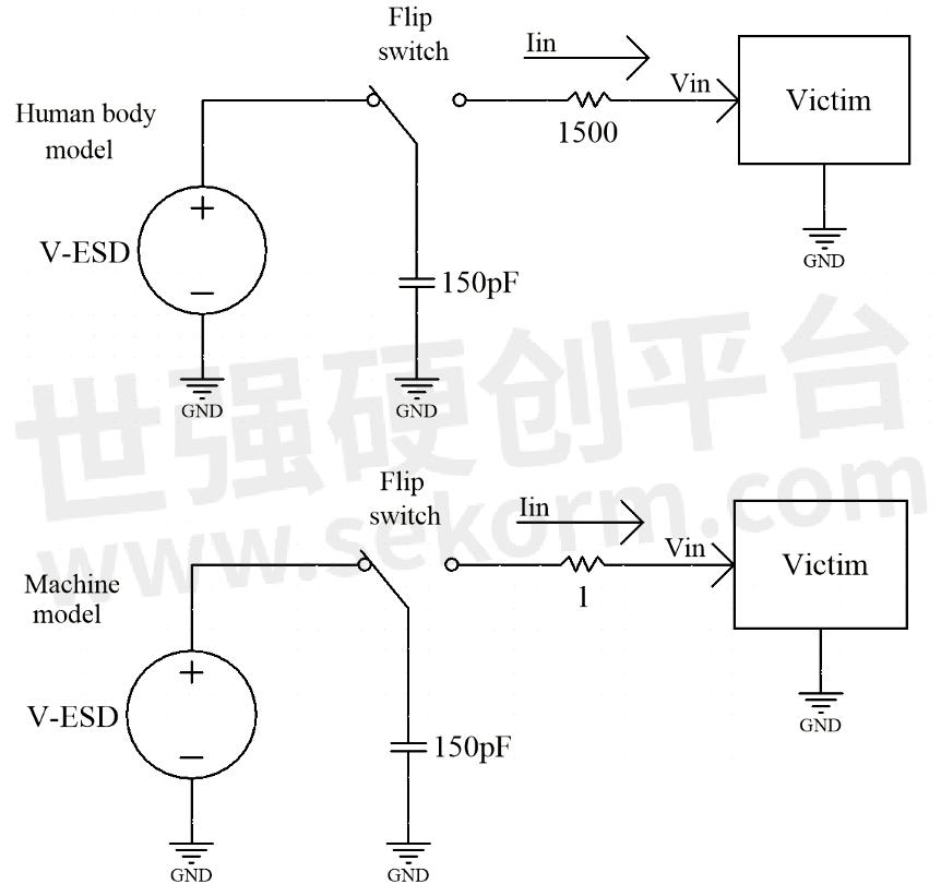
Figure 1: Board-level ESD typically involves machine model (MM) and human body model (HBM)
High transient voltages that destroy damaged circuits generally have a rise time of a few nanoseconds and a discharge time of about 100 nanoseconds. Different circuits are damaged, and their susceptibility to positive and negative shocks can also be very different, so you need to deal with both Good positive and negative impact. The difference between the two most common models, the Human Body Model (HMB) and the Machine Model (MM), is primarily in series resistance. Mannequins are not as conductive as metals.
The best protection against overvoltage damage is voltage limiting or clamping with nonlinear circuits (Figure 2). The most commonly used are specialized diodes, which have very low impedance when they are forward biased or in the Zener breakdown region. Introducing a voltage limiter can quickly cause something else to happen because there is a large inrush current through the voltage limiter through the discharge of the capacitor.
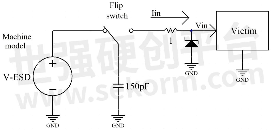
Figure 2: A basic voltage limiting circuit can prevent overvoltage damage
Although high transient voltages are eliminated, replacing them with inrush currents of several amps can cause other problems in the system. Depending on the total impedance of the subsequent path, the inrush current can reach several amps. When designing I/O cells for chips, it is common to see inrush currents of 4A to 16A entering the device. Handling such huge transient surge currents has become a big problem in ESD design. Limiting the voltage is relatively easy, but the resulting current can reverse circuits and grounds elsewhere in the system.
The current forced into the ground by the voltage limiter will cause inductive ringing in that node of the system (Figure 3). Power usually travels along the ground wire and is a function of the power supply decoupling capacitors so the system core can still function properly. However, the control lines going to the board can be confusing because they are established relative to the ground off the board. The result could be an ESD event somewhere and cause an input on the board to appear to be faulty.
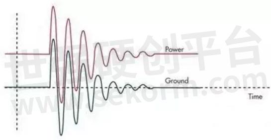
Figure 3: Injecting a large inrush current through a voltage limiter into the ground causing the PCB ground
bounces and behaves as a function of the connection inductance
The role of fortresses
With board-level ESD, you can try to build a fort with multiple controlled access points on the "moat". Connections beyond the "wall" can be broadly divided into several categories: protocol-controlled data, low-bandwidth detection and control lines, and high-speed interfaces. The first two are relatively easy to handle, and the third is somewhat challenging. There are several different ways to protect these three parts from ESD damage.
Regardless of the final product, some form of protective casing will be part of the device. Isolating the circuits inside the enclosure is the first line of defense that requires careful consideration. Ideally, a metal case to connect the circuit board would usually work, but modern products often use non-conductive plastic or other modern materials.
Circuit designers often have no control over the materials used to build the walls, but have an inescapable responsibility for protecting the fort. When designing an enclosure, care needs to be taken that ESD reaching any part of the exterior of the enclosure will have countless paths to the internal circuitry.
Building a PCB that is self-protecting against ESD strikes can start with low-impedance grounding methods. Establishing a foundation and normal power integrity allows the printed circuit board (PCB) to maintain signal integrity across the board, even when subjected to large ground surge currents.
As a design engineer, you would ask everyone to fasten their seat belts, which can deal with a small amount of airflow. The plane may bob up and down quickly, but if everyone is wearing their seat belts, everyone will stay in place and the plane will continue to fly. After this, you need to protect the external connections and limit the effects of ESD events.
The protection circuit should be located at the entry point of the board, not downstream of the entry point. It could be thousands of volts of potential caused by arcing issues to deal with, or inrush currents of several amps that are best handled at the edge of the board.
TVS voltage limiter
Transient Voltage Suppression (TVS) limiting diodes can be used as voltage limiters. They are divided into common voltage, logic level and supply voltage. Common voltage types are: 12V, 5V, 3.3V, 2.5V, 1.8V and 1.2V.
This number should look familiar, as these devices are specifically designed for the requirements associated with many CMOS devices. One size cannot meet all requirements, they should be the correct voltage for the device to be protected.
It is worthy of our respect that modern CMOS processes have significantly reduced supply voltages to protect transistors that do not have a lot of design margin and have a limited voltage range. These devices are typically fabricated using foundry processes that provide high current devices with low impedance characteristics in small packages.
Placing a TVS voltage limiter on the input line protects the input from destructive ESD damage (Figure 4). But this voltage limiter cannot handle the signal chaos that occurs when the host is processing it, nor can it handle the reversal effects that occur due to huge ground current surges.
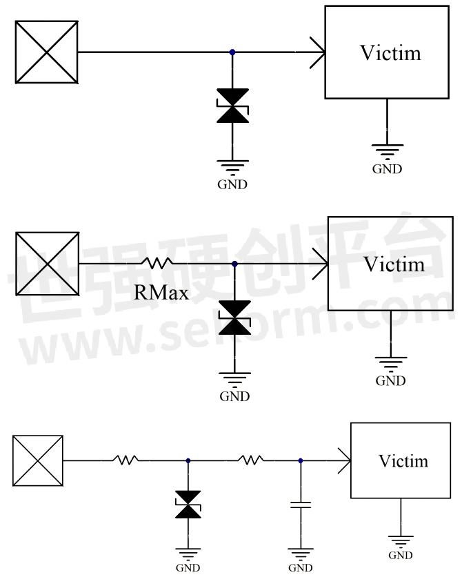
Figure 4: Simple voltage limiting can provide overvoltage protection, but can cause inrush current problems.
The inrush current should be limited and the signal should remain relatively local ground stable.
As mentioned earlier, the performance difference between HBM and MM is very large. In many cases, adding some series resistance before the TVS device can help limit current surges and reduce ground bounce. As with HBM, the end result is reduced system stress.
Usually, bandwidth limitation alone will not solve the ESD problem. The low-pass filter also requires 60dB to 150dB of attenuation for small ESDs to eliminate transient voltages, which is difficult for simple passive filters. The TVS voltage limiter can pull the signal down between the power rails.
A first-order RC circuit can then be used to maintain signal integrity (Figure 4). Capacitors can also stabilize the input voltage with respect to local ground. This approach works well to protect a large number of low-bandwidth inputs, including "set-and-forget" control lines, sensor inputs, and the like.
While most of our discussion is about protecting the input ports of a PCB, output port protection is similar. TVS voltage limiters and additional resistors would also be appropriate here. Limiting the voltage helps prevent damage to semiconductors and protects other components that have voltage limits.
The series resistance also contributes to ground stabilization. In addition, keeping the ESD surge current away from the digital chip's I/O cells prevents ground bounce inside the chip, allowing the processor to remain functional while an external voltage limiter absorbs the surge current.
ESD inside the chip
The ESD protection capabilities within an IC are somewhat compromised for a number of reasons. Both silicon and metal are optimized for the core functions of the IC and are not suitable for high current operation. Specialized TVS devices use silicon wafers optimized for high-current circuits and have higher performance than PN junctions in common CMOS.
In addition, I/O cells with high-current ESD protection can take up considerable space, driving up IC costs. Also, high-frequency pins on an IC usually cannot have large-scale ESD protection circuits attached because they create capacitive loads.
As a general rule of thumb, the level of ESD protection inside the chip is only sufficient to complete the IC production and soldering to the PCB, but it lacks the robust protection performance typically required by the application environment. If the connection needs to leave the PCB, further protection is usually required with external devices.
Recommended Products
In response to the problem of ESD protection inside the chip, the ICW3490E product of Hefei Aichuang Microelectronics Technology Co., Ltd. uses the ESD design technology, and realizes the ballast resistance through the efficient area use method, which can ensure the realization of smaller I/O and smaller IC chip size. The design method consists of a back-end ballast (BEB) with a segmented device design, an integrated ballast circuit (MBC) layout, and a multi-contact circuit design (MFT). Compared with traditional process technology, the combination of BEB, MBC and MFT in typical 0.18μm process technology can improve ESD performance by more than 60%; voltage clamping efficiency by more than 30%; on-resistance improved by 50%; area efficiency The improvement is 2 to 3 times. This technology not only provides high ESD performance, but also does not require silicide modules.
The ICW3490E is a 3.0V~5.5V power supply, full duplex, low power consumption RS-485/RS-422 transceiver that fully meets the requirements of the TIA/EIA-485 standard. The ICW3490E includes a driver and a receiver, both of which can transmit signals independently. The ICW3490E has a 1/8 load, allowing 256 ICW3490E transceivers to be connected in parallel on the same communication bus. Error-free data transmission up to 14Mbps can be achieved. The working voltage range of ICW3490E is 3.0V~5.5V, and it has functions such as current limiting protection, overvoltage protection, and hot-swap input of control ports. ICW3490E has excellent ESD release capability, HBM reaches ±15KV.

Figure 5: ICW3490E pinout diagram
Data communication port
A properly designed communication port uses a robust protocol that includes a common use of Cyclic Redundancy Check (CRC) encoding to test data integrity. Ethernet, USB, and CAN buses have all developed CRC codes and sent them along with the data. A properly designed receiver will check that the CRC encoding matches the data being sent. If it does not match, it means that either the data or the CRC encoding has an error, and a request to resend the data will be issued.
Because ESD events last less than 100ns, the CRC check, verification, and resend process typically invisibly handles ESD. End users generally never realize that corrupted information has been corrected. Some other protocols have no protection in their structure.
The I²C, Serial Peripheral Interface (SPI), and System Management Bus (SMBus) communications are designned to work on the PCB and cannot verify and correct data. If some data is going to leave the board, make sure you have a way to verify the validity of the data.
Most modern communication paths are differential, using some form of low voltage differential signaling (LVDS). Every LVDS connection needs to be TVS protected like all other signals. Magnetic field isolation (common in Ethernet) and common mode chokes help address common mode variations due to ground bounce during ESD events. When the input signal and the PCB do not share the same ground, optical isolation or magnetic isolation measures should be taken.
High-speed data streams that require perfect data integrity but do not include error checking are particularly difficult to protect against ESD strikes. Understanding how the device provides serial data rates above 1GB/s and full communication protocol protection can avoid this problem.
Analog Signals and Digital Intelligence
Basic TVS protection is required for any analog signal leaving or entering the board. The bandwidth of the connection channel needs to be considered to determine what other actions should be taken next. Most analog control signals, motion control systems, audio and indicator lights require no further measures because of the longer response times of the devices used. The RF front end is the physical layer of the communication channel, and self-correction is provided by error detection mechanisms that are part of the protocol.
Hardware can only provide so much protection. If a processor in the center of the system needs to do monitoring and control, then some options are also required. The techniques described here will keep your processor from losing, or going through a reset cycle. What exactly happens under the control of this host is another matter to consider.
Generally speaking, you need to build some intelligence into the processor code so that it can recognize incorrect information and handle it correctly. The slow detection and control line problems can be easily solved by polling the port by time division. Since ESD events are very brief, if the data on the port remains stable for multiple samples within a few milliseconds, the system is free from catastrophic events such as ESD.
Also, the output can be refreshed as part of the reproduction process. This step is not needed if the processor is a memory unit, but if the data is locked remotely, a refresh routine is needed to manage corrupt events.
- +1 Like
- Add to Favorites
Recommend
- Principle and Application of Linear Regulator LDO
- The Lithium Battery Market Is Growing Rapidly, and The Demand for Management Chips Is Strong!
- What Is LED Driver Power Supply?
- Syrlinks Releases a New Generation of S-Band Transceiver EWC31-NG For Small Satellites,Delivering Low Power Consumption and Radiation Tolerance
- CW32 is a Low-power 32-bit Microcontroller, Using Arm Cortex-m0+core, Very Suitable for Intelligent Temperature Controllers with Low Power Consumption Requirements
- What is Low power consumption Bluetooth module?
- Renesas Unveils RAA270205, the First 4x4-channel 76-81GHz Automotive Radar Transceiver with High Accuracy and Low Power Consumption
- LoRa®-Based Solution from Renesas to Develop IoT Applications with Low Power Consumption
This document is provided by Sekorm Platform for VIP exclusive service. The copyright is owned by Sekorm. Without authorization, any medias, websites or individual are not allowed to reprint. When authorizing the reprint, the link of www.sekorm.com must be indicated.
Integrated Circuits


Discrete Components


Connectors & Structural Components


Assembly UnitModules & Accessories


Power Supplies & Power Modules


Electronic Materials


Instrumentation & Test Kit


Electrical Tools & Materials


Mechatronics


Processing & Customization


