An Introduction to Semiconductor Device Modeling

In the semiconductor IC design field, packing over 1 trillion transistors in a single processor is becoming the standard. With the process technology advancing toward 2 nanometer (nm) process nodes and lower, smaller device sizes introduce additional unforeseen effects at the nanoscale, uncharted in older technologies.
Accurately modeling such semiconductor devices is becoming increasingly complex each year. Engineers must determine hundreds of parameters to accurately predict the behavior of these devices across various sizes and temperatures. To deliver high-quality semiconductor designs faster, engineers need powerful device modeling tools.
In this article, you’ll learn about modern device modeling and its challenges. You’ll gain an understanding of device modeling flow, the role of device modeling in the design process, what goes into a device model, and which device models and modeling tools are available.
What Is Device Modeling?
Device modeling is the creation of mathematical models and formulas that describe the characteristics and behaviors of semiconductor devices, under different operating conditions.
The characteristics include:
· Electrical properties like voltages, currents, and capacitances under direct current (DC) and alternating current (AC) signals
· Electromagnetic (EM) and radio frequency (RF) characteristics like S-parameters and noise
The behaviors include phenomena like semi-conduction, thermal, and quantum effects.
Why Is Semiconductor Device Modeling Important?

Semiconductor devices are getting increasingly complex. Complex ICs like systems-on-a-chip (SoCs) and extreme miniaturization like the three-nanometer process are becoming common. These introduce a variety of complications like noise and heating.
To cope with such complex requirements, engineers use device modeling software to thoroughly understand, predict, and optimize the behaviors of devices.
This provides the following enormous benefits to device makers:
· Satisfies complex requirements: Device modeling helps engineers simulate different operating conditions and optimize their designs.
· Reduces costs: Each spin cycle (i.e., a round of design and fabrication) incurs higher fabrication costs. Virtual iterations are far cheaper.
· Shortens the time to market: Spin cycles also mean a longer time to market. Device modeling enables fast iterations with incremental improvements.
· Increases reliability: Device modeling confers long-term reliability, which means satisfied customers.
Which Semiconductor Devices Are Modeled?
Some of the common semiconductor devices that are analyzed using device modeling tools include:
· Various field effect transistors (FETs) like metal-oxide-semiconductor FETs (MOSFETs), junction FETs, and FinFETs
· High electron mobility transistors (HEMTs) like gallium nitride HEMTs (GaN HEMTs)
· Bipolar junction transistors
· Complementary metal oxide semiconductor (CMOS) devices
· Very large-scale integration (VLSI) devices like amplifier ICs and SoCs
· Transferred electron devices
· Diodes
· Integrated passive elements
Who Publishes Device Models, and Who Uses Device Models?
Companies that design such semiconductor devices use device modeling techniques extensively and provide their device models to customers. Many design companies are fabless — they don't do the physical fabrication themselves but outsource to foundries like TSMC. Others are integrated device manufacturers (IDMs) that design as well as fabricate.
At a higher level, system integrators are companies that target particular applications and industries by building circuits and equipment consisting of semiconductor devices. They use the device models from device companies in circuit simulation software like SPICE (Simulation Program with Integration Circuit Emphasis).
The Role of Device Modeling in Device Design
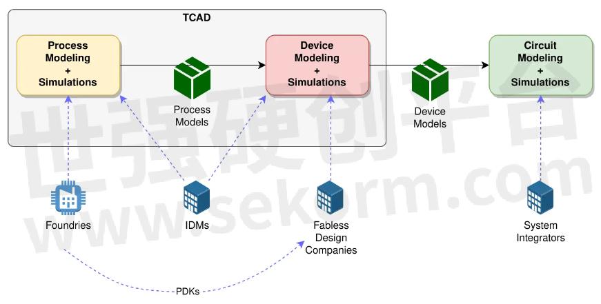
In this section, we'll first give a high-level overview of where device modeling fits in the overall design process when using electronic design automation (EDA) and its subfield, technology computer-aided design (TCAD). We go into more detail in later sections.
Process Modeling and Simulation
In the process modeling phase, the fabrication processes for the planned device are simulated and optimized virtually using TCAD software like process simulators.
These tools enable virtual fabrication. They can simulate steps like doping, etching, deposition, and oxidation, which alter the structural and chemical properties of the material layers. Process modeling predicts the resulting impurity profiles, layer thicknesses, and wafer topographies after each process step.
In the case of fabless designers, fabrication foundries do most of the process modeling and provide their manufacturing process models as process development kits (PDKs) to help designers meet device performance, power, and area targets quickly.
However, IDMs often do the process modeling themselves since they fabricate in-house, especially when using proprietary techniques based on their intellectual property.
Device Modeling and Device Simulation
In the device modeling phase, the goal is the mathematical characterization of the physical, electrical, thermal, and other behaviors of the device.
Device designers do most of the modeling and simulations and produce the device models for their customers. Some of the models and parameters from the previous process modeling are used in this phase.
Circuit Modeling and Simulation
In this phase, circuit designers in system integrator companies seek to understand how their circuit behaves under different operating conditions. Some of the device models that are optimized for simulation are used with circuit simulation software like Advanced Design System (ADS).
Types of Device Models
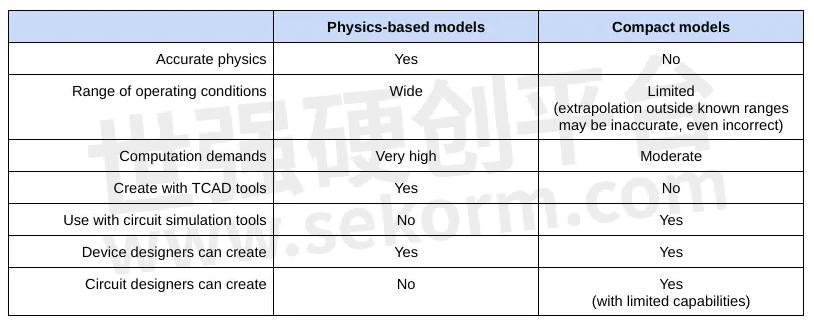
The device modeling phase can produce three types of models:
· Physics-based models: They're useful for exploring new device architectures or new materials by simulating semiconductor, quantum, thermal, EM, and RF phenomena.
· Compact models: They're used in high-level electrical simulations of integrated circuits and circuit boards. Some are derived from or simplified versions of physics-based models. Others are empirically determined from experimental data.
· Artificial neural network (ANN) models: For complex devices like thin-film transistors, memristors, or photonics semiconductors, compact models may take weeks or months to become available and may not have the desired level of accuracy at first. You can alleviate those problems by quickly training empirical, nonlinear ANN models instead of using a fully automated pattern extraction process. Such ANN models predict desired output parameters (like drain voltages) by learning the hidden patterns in high-dimensional, high-volume data consisting of dozens or even hundreds of measured parameters, like I-V, S-parameters, gate voltages, drain voltages, temperatures, and so on.
In general, physics-based models have better scalability for various operating conditions. Other differences are depicted below:
Physics-Based Device Modeling
In the design modeling and simulation phase, device designers focus on the physics-based modeling of:
· Properties of semiconductor materials (silicon or III-V compounds), like bandgap, electron mobility, Fermi levels, and dielectric constants
· Carrier generation and recombination
· Transport mechanisms like drift, diffusion, and tunneling
· Effects of layer dimensions and geometries
· Boundary conditions at substrate and other interfaces
· Nanoscale quantum mechanical effects
· Thermal behavior
· Polarization behaviors of direct bandgap semiconductors used in optoelectronics
· Effects of manufacturing parameters from the previous process modeling phase
TCAD vendors implement these mathematical models in their software with the necessary front-end and backend support. Device designers incrementally refine their models by iterating these steps:
· Device designers enter all the specifics and dimensions of their proposed designs.
· The TCAD software simulates the phenomena over time or under various environmental conditions using techniques like finite element methods.
· The calculated model parameters, results, and graphs are analyzed against experimental or ideal data.
· Any design issues or optimization bottlenecks are addressed by tweaking the proposed design, and the steps above are repeated.
Compact Device Modeling
Compact device modeling produces simplified empirical models that are useful for understanding the electrical behaviors of the device and can be used directly in electrical circuit simulations.
They may be simplified versions of physics-based models and also incorporate parameters from the process models.
Compact models typically contain a core set of models and formulas for predicting, under various operating conditions, the device's electrical properties like:
· Current-voltage (I–V) characteristics and curves
· Capacitance-voltage (C–V) properties and curves
· DC characteristics
· AC characteristics
· Time-domain transient behavior
· Models for parasitic capacitances and resistances
· RF-related properties like S-parameters
· Leakage currents
In addition, they model a variety of physical phenomena that are required for accurately simulating electrical behaviors based on theories and equations like:
· Poisson's equation of electrical fields
· Conductivity equations
· Boltzmann transport equation
· Shockley-Read-Hall recombination theory
· Empirical formulations like the Van Overstraeten avalanche model
Compact Modeling Techniques
Compact models are generally created in two ways depending on who's doing the creating.
1. Measurement-based models
These are created by designers or full-time modelers in the device company. They have measurement equipment to experimentally test their designs, fit their device models to the experimental data, and perform model extraction to infer unknown parameters. Such models are more detailed because they are created by the designers themselves. Their accuracy is higher because they're adjusted to match experimental data using optimization algorithms.
A key challenge here is that DC C-V and RF modeling of semiconductor devices require a significant amount of measured data from different wafers over several temperatures that must be collected efficiently and with high accuracy. Good RF calibration and de-embedding of instruments, cabling, and probes are essential.
If the number of parameters is high, artificial neural networks can be used to create accurate nonlinear empirical models. For example, the NeuroFET model learns device behaviors across a range of biases, frequencies, and other parameters based on DC and S-parameter measurements with minimal degradation and predicts parameters like the current and charge constitutive relations.
2. Target-based models
Concurrent design has become increasingly common to reduce the time to market. IC device models are sought to be extracted even before their manufacturing techniques have matured and stabilized. Many device models are now extracted not from measurement data but based on projected device characteristics known as targets. These techniques are called target-based or speculative model extraction.
Target-based modeling offers significant competitive advantages for design houses:
· The ability to customize foundry-provided SPICE libraries to device targets derived from internal design specs significantly speeds up the modeling and design iterations.
· Although foundry models have evolved significantly and achieved impressive quality overall, they may still fall short on some applications that weren't foreseen or characterized during extraction. Target-based models enable overcoming such model deficiencies.
3. Datasheet-based models
These are ad-hoc models created by circuit designers when proper device models are not created or provided by the device company. They're empirical models created by fitting the curves found in the device's datasheets.
Compact Models for Analog and Digital Circuits
Most modern ICs are a mix of analog and digital circuits and signals. So tools support various modes like analog, digital, mixed-mode, and RF simulations.
To integrate properly with simulators, modern device models also support all these simulation modes. For example, the EKV3 model of a CMOS transistor supports all these modes.
Examples of Compact Device Models
For a better understanding of device models, we briefly explain two simple, example device models below. However, most devices are more complex than this and require more complex models like the standard models described later.
Device Model of a Bipolar Transistor
The illustration below shows the physical semiconductor structure of a transistor and its equivalent circuit proposed by the Gummel-Poon model.
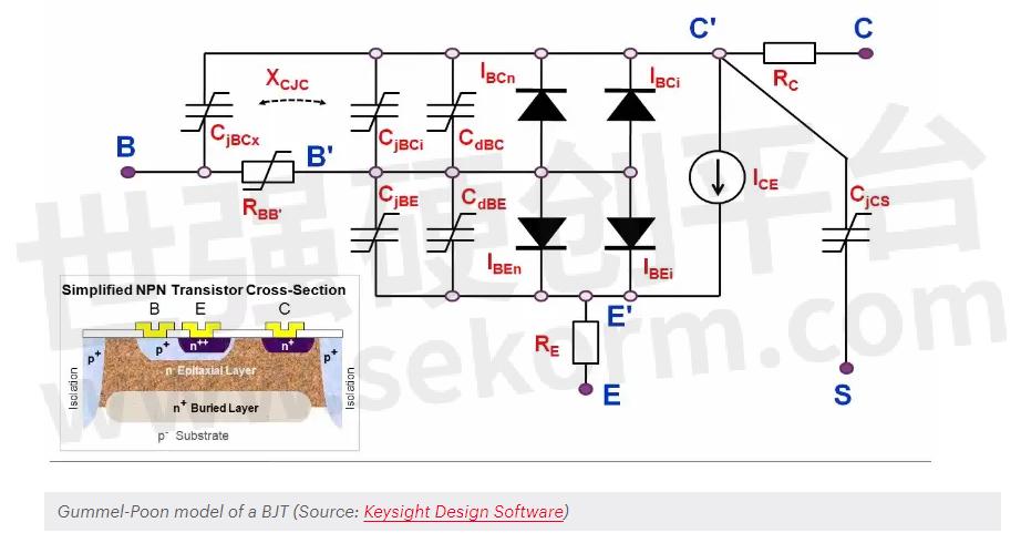
Such a model enables the following key capabilities among others:
· It gives equations for the currents in each region for I-V modeling.
· For C-V modeling, it gives equations for the junction capacitances.
· It enables accurate modeling over a variety of operating conditions by formulating physical phenomena like the Early effect of base-width modulation, the Webster effect, the Kirk effect, and more.
Device Model of a MOSFET
The illustration below is related to the physics-based device modeling of an n-channel MOSFET.
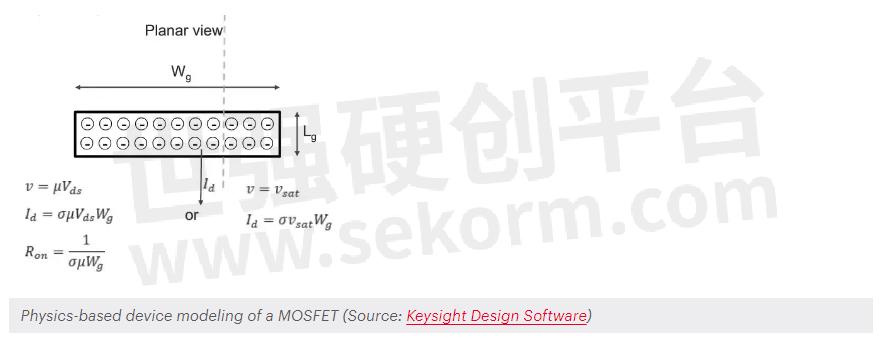
Such models use fundamental equations like Poisson's equation to determine characteristics like:
· Area charge density
· The electric field across the gate with an oxide insulator
Compact empirical models for MOSFETs — like the Berkeley short-channel IGFET model (BSIM) family — are based on these physics-based models. The BSIM models are optimized for fast circuit simulation and refined to fit real-world experimental measurements by adding parameters. They enable circuit designers to characterize MOSFET electrical behaviors using properties and parameters like:
· I-V and C-V characteristics
· Drain-source voltage, Vds
· Threshold voltage
· Gate capacitances
· Bulk threshold parameter
· Layer dimensions like the gate oxide thickness
Standard Compact Models
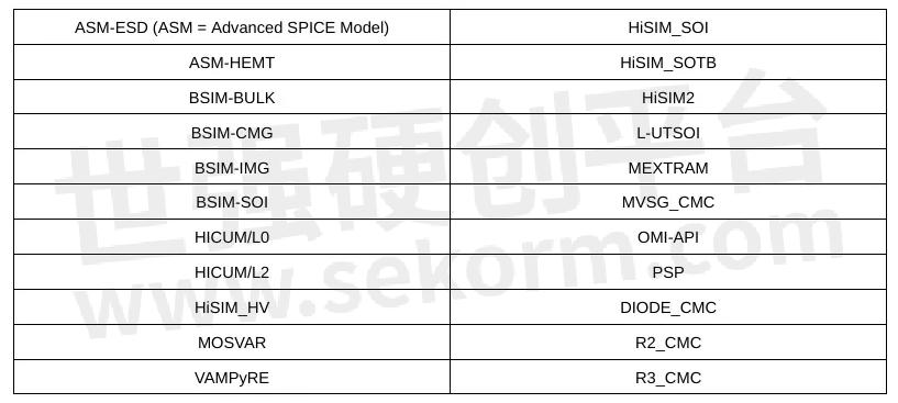
Standardization of compact models enables all stakeholders to agree on the same modeling theories, equations, model parameters, mathematical attributes, definitions, and names. This facilitates the interoperability of different device designers, foundries, system integrators, and modeling/simulation software from different vendors.
The Compact Model Coalition (CMC) is a standards body that publishes a set of standard models for various devices. Some of the standard models are shown below.
Take a Look at Keysight’s Device Modeling Products and Services
Keysight offers a comprehensive set of EDA software and services for all stakeholders:
· PathWaveDevice Modeling (IC-CAP) is a keysight core, modular platform for device modeling.
· PathWave IC-CAP add-on packages add a variety of device models like GaN HEMT, GaN RF, power electronics, and more.
· PathWave Model Builder is a model extraction software with macro-modeling, Verilog-A support, and advanced fitting and optimization techniques.
· PathWave Model QA is a model validation tool.
· PathWave Advanced Design System is an advanced circuit design and simulation software with add-on bundles for specific analyses like electromagnetic, electro-thermal, or RF, and specialist industries like power electronics.
· PDKs of popular foundries are available for ADS.
In addition, Keysight provides device modeling services and special support services for EDA products.
- +1 Like
- Add to Favorites
Recommend
- Unveiling the Latest Innovations in Keysight EDA Software
- Keysight Expands EDA Software Portfolio with the Acquisition of Cliosoft
- Keysight Joins TSMC Open Innovation Platform 3DFabric Alliance, Accelerating EDA Software and Testing Solutions Development
- Keysight Introduces PathWave Design 2024 with Automation and Collaboration Support for Enterprise EDA Workflows
- Julin Technology Attended Elexcon 2023 with Independently Developed and Designed EDA Simulation Software
- Keysight EDA 2024 Integrated Software Tools Shift Left Design Cycles to Increase Engineering Productivity
- Cloudification of Test Software,Keysight Open RAN Architect (KORA) software is available on AWS
- Keysight Introduces QuantumPro Delivering First Integrated EDA Workflow for Qubit Design
This document is provided by Sekorm Platform for VIP exclusive service. The copyright is owned by Sekorm. Without authorization, any medias, websites or individual are not allowed to reprint. When authorizing the reprint, the link of www.sekorm.com must be indicated.
Integrated Circuits


Discrete Components


Connectors & Structural Components


Assembly UnitModules & Accessories


Power Supplies & Power Modules


Electronic Materials


Instrumentation & Test Kit


Electrical Tools & Materials


Mechatronics


Processing & Customization


