Unveiling the Latest Innovations in Keysight EDA Software
As the landscape of electronic system design evolves, design engineers developing high-speed, high-frequency products in multiple applications need to stay updated with advanced electronic design automation (EDA) tools. Keysight's EDA Software, as one of the leaders in this domain, continually introduces new features that transform the design, simulation, and analysis processes.
In this comprehensive blog post, we will guide you through the latest innovations in Keysight EDA, emphasizing how these developments can significantly enhance your shift-left strategies and engineering productivity.
Maximizing Shift-Left Strategy with Top 6 Upgrades in Keysight EDA Software
Keysight EDA offers a seamless and integrated experience for electronic design, from initial design and simulation to validation and manufacturing. With its latest updates, the platform has introduced a range of new features that cater to the industry’s ever-evolving needs.
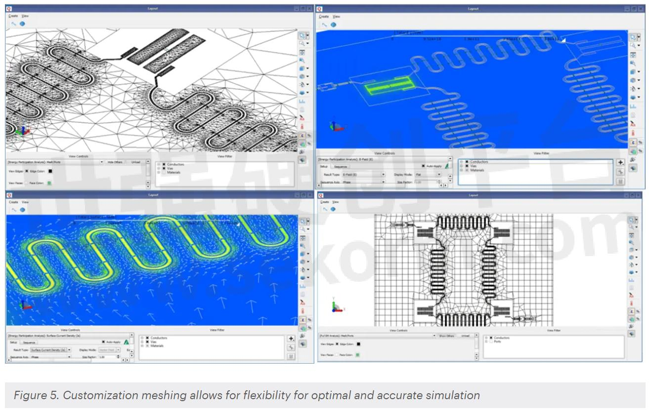
#1 Advanced simulation technologies
The latest versions of EDA software bring enhanced simulation capabilities for radio frequency integrated circuits (RFIC), electromagnetic (EM), electro-thermal analysis, and more. These improvements, powered by industry-leading measurement science, allow for more accurate and faster simulations, enabling engineers to shift left design validation more efficiently in the product development lifecycle.
#2 Enhanced integration with other tools
Given the importance of interoperability in today’s design workflows, Keysight has focused on improving the integration of its EDA software with other popular design and simulation tools. The integration of Python APIs enables engineers to leverage the best features of each tool and automate their workflows, significantly reducing manual effort and minimizing human error. A prime example of this is the repeated electromagnetic (EM) extraction for printed circuit boards (PCB) in high-speed digital signal designs, performing channel simulation on the resulting EM model, and invoking digital standard compliance tests, in one automated process.
#3 Expanded libraries and component models
The new versions of EDA software include expanded libraries and component models, offering designers a broader range of elements to incorporate into their designs. This addition is particularly beneficial for those working on cutting-edge projects that require the latest components.
#4 Advanced analytics and optimization tools
With the integration of advanced analytics and optimization tools, Keysight EDA software enables engineers to extract deeper insights from their designs. The advanced tools assist in identifying potential issues early in the design process and suggest optimizations for enhanced performance.
#5 Improved user interface and experience
The updated software features a more intuitive user interface, making it easier for designers to navigate and utilize the various tools within the suite. This enhancement streamlines the design process, reducing the time and effort required to achieve successful results.
#6 Cloud-based collaboration features
In response to the growing trend of remote and distributed work, the latest updates include enhanced cloud-based collaboration features. This includes a new Design Cloud use case for parallel simulation supporting electrothermal (ETH) simulation for RF power amplifier design to achieve broader coverage of temperature corners in a shorter period. These features enable design teams to work together seamlessly, regardless of their physical location.
A Deep dive into new features and enhancements
Keysight EDA offers solutions for various applications, including wireless communication, high-speed digital systems, and device modeling. Its versatility makes it appropriate for different applications, from small-scale IoT devices to large, sophisticated systems, ensuring high precision and efficiency in electronic design processes. Here are some examples.
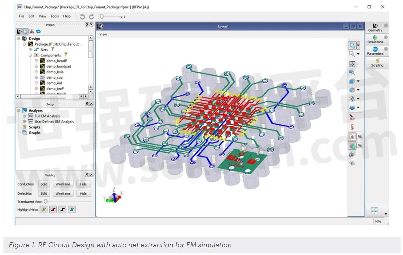
RF & microwave design advances
Keysight's newest RF and Microwave design tool updates focus on enhancing simulation accuracy and speed. These improvements are engineered to enable multi-technology (RFIC, MMIC, antennas, packaging, PCBs, etc.) assembly and 3D EM-circuit-electro-thermal co-simulation, helping engineers tackle complex design challenges in radar, communication systems, and RF circuits.
Moreover, new Python scripting opens the RF/Microwave design platform for flexible custom capabilities, automation, and integration in multi-tool enterprise design flows. In particular, users can now access the Python-based Artificial Neural Network (ANN) modeling framework from Keysight's proprietary DynaFET to build their own nonlinear circuit simulation models faster while dramatically increasing simulation coverages. Integrating new models and more sophisticated analysis methods provides a significant edge in developing cutting-edge RF solutions.
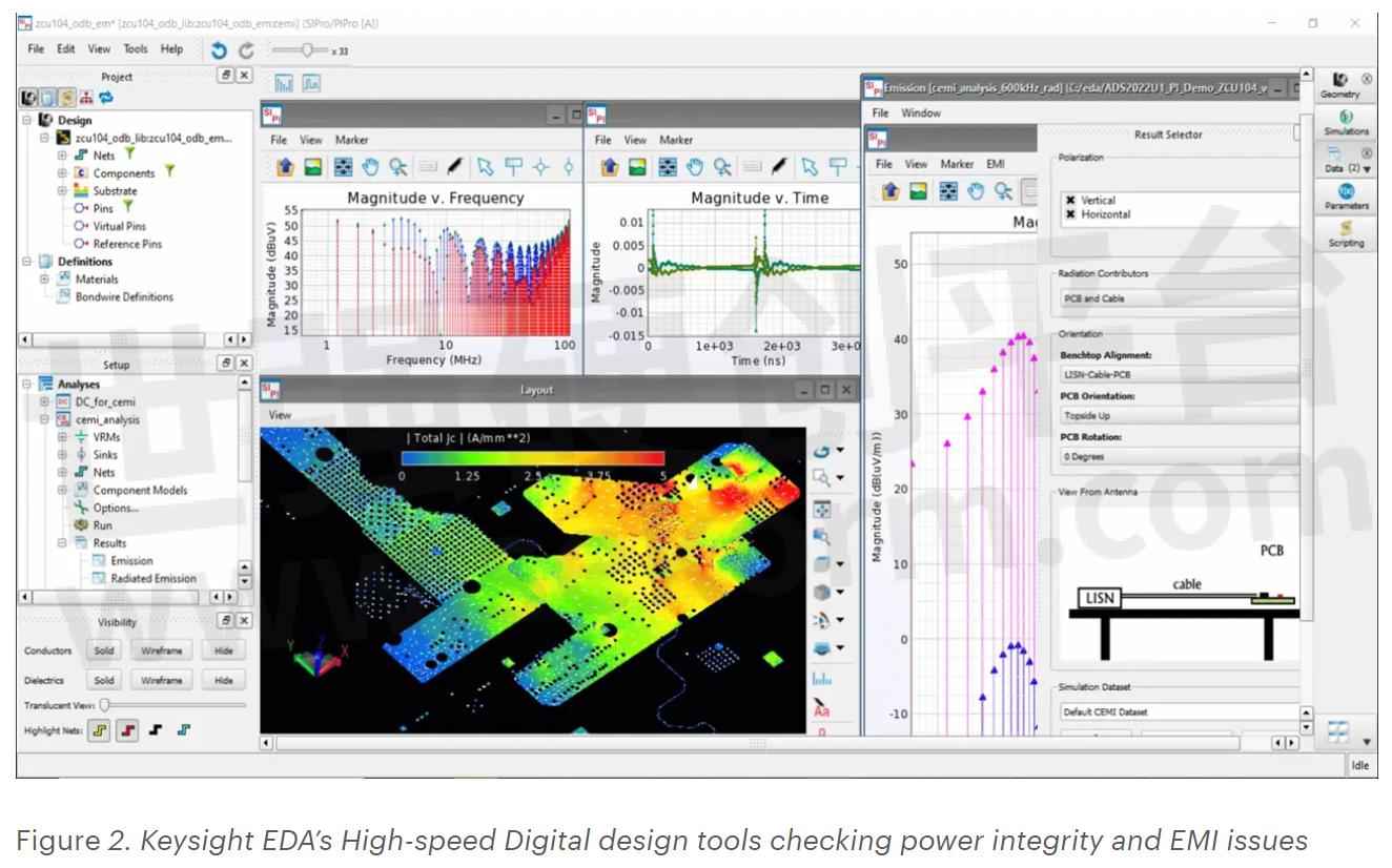
High-speed digital developments
High-speed digital design demands precision and efficiency. Keysight's updated EDA software for high-speed digital applications introduces advanced signal integrity analysis, thermal management, and power integrity features. These tools are crucial for engineers working on high-performance computing, networking, and data center technologies.
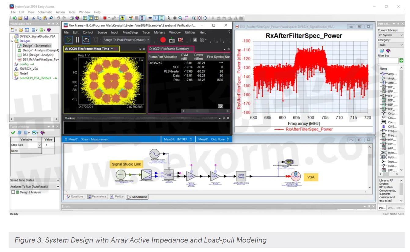
RF system design innovations
As one of the industry's leading electronic system-level (ESL) design environments, Keysight EDA's system design introduces significant enhancements for a seamless experience from concept to product, such as the integration of system and circuit design workflows, enhanced power amplifier modeling, advanced Satcom design features, and AI/ML models integration for the advanced 5G air interface. The latest updates offer improved modeling capabilities, better system-level verification, and more comprehensive co-simulation options. These features streamline the development process for complex systems.
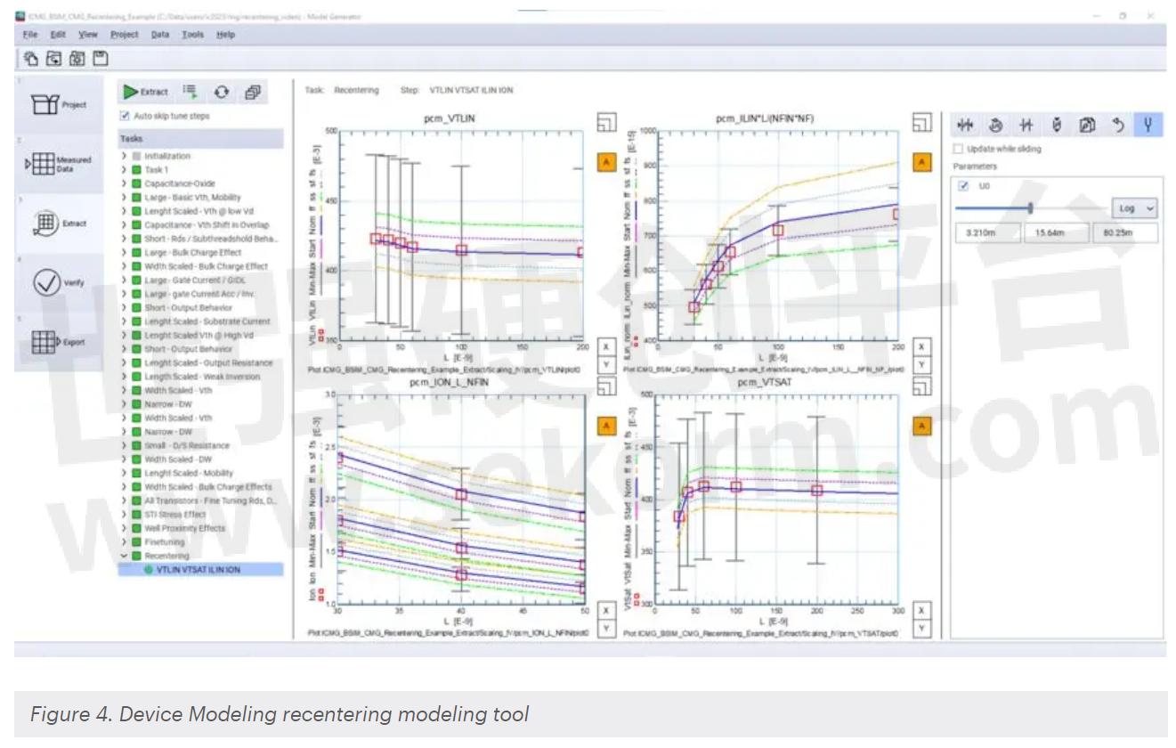
Device modeling enhancements
Accurate device modeling is critical for successful semiconductor design. Keysight EDA's recent updates in the device modeling and characterization products comprise a new recentering modeling tool, automated model extraction solutions, one-click model qualification, and integrated, advanced low-frequency noise analysis.
These enhancements support a wide range of semiconductor devices and materials, aiding in developing more efficient and powerful electronic components. For example, model re-centering can reduce the modeling extraction time by as much as 70% compared to traditional step-by-step extraction flow.
Advanced power electronics design
Keysight continues the innovation that has made it one of the industry’s most trusted Power Electronics (PE) EDA software tools. The new features in power electronics modeling extend thermal analysis at the board and schematic level, allowing PE engineers to:
· Analyze hot spots on their PCB via a graphical heat map
· Compute power losses and estimate junction temperatures on the schematic design
Other updates such as the new switched-mode power supply (SMPS) performance test bench and the IGBT model extraction focus on simplifying the design and analysis of power electronic systems, including converters and inverters. PE engineers can more accurately predict system behavior under various conditions with enhanced simulation capabilities.
EDA solutions for quantum computing
Quantum computing is a rapidly emerging field, and Keysight stands at the forefront of it with Quantum EDA solutions. QuantumPro is one of the industry's first integrated workflows tailored for the seamless design of superconducting qubits.
Our solutions help engineers explore new quantum computing technologies from superconducting qubits to quantum amplifiers with first-in-class simulation and analysis capabilities. For example, the nonlinear circuit solver delivers a comprehensive analysis of the power-dependent performance of the quantum chips, enabling the designers to analyze and optimize their quantum chips quickly. Besides, we have included an alpha feature for a Python console that enables easy control of workflows, workspace modification, automated tasks, and customizable user interfaces.
AI and machine learning for EDA software
Incorporating AI and machine learning in EDA tools marks a significant step forward. We’ve enhanced the AI/ML capabilities into the latest release to solve emerging design challenges – for example, using ANN model for RF simulation, eye diagram estimation, channel modeling for pre-6G system simulations, and ANN modeling of GaN devices with memory effects. These technologies offer predictive analysis, optimization capabilities, and intelligent decision-making support, enhancing the efficiency and effectiveness of the design process.
Python for EDA
Automation and API-based workflows are a cornerstone in digital transformation. Recognizing the importance of agility and flexibility in today's engineering tasks, Keysight has integrated Python scripting capabilities into its EDA software to streamline post-processing simulation data, automate repetitive tasks, and increase design-to-test efficiency. There are various application examples of Python APIs.
1. Custom workflows: Automate tasks such as data manipulation, data visualization, and sophisticated layout and PDK objects; perform complex batch simulations; create netlists or edit model parameters; and create custom applications & GUIs.
2. Loadpull data import: Connect “Data Islands” into workflows by generating new value from existing data; enabling flexible import/conversion of a variety of data formats and irregular data; and unifying tasks across multiple tools & processes
3. ANN modeling: Turn data into executable models with smoother, continuous interpolation from sparse, irregular, or multi-dimensional data; faster behavioral execution; better-protected IPs; and transportable digital twinning
4. Direct test connections: Bring test and measurement into the design processes with links to PNA and VSA-VSG

Accelerating semiconductor innovations with Keysight EDA
In an era where semiconductor and electronics industries are grappling with increasing complexities and the pressure to speed up product launches, engineering leaders are in dire need of solutions that enhance design productivity.
Keysight's EDA software suite, constantly evolving to address the modern challenges faced by engineers and designers, offers streamlined tool workflows, facilitates global sharing of extensive design and simulation data, and digitizes all facets of development programs. By integrating these cutting-edge features into your workflow, you can gain a competitive edge in electronics design and analysis, ensuring faster, more reliable market entries.
Explore these innovative solutions more at Keysight EDA – claim your free trial today!
- +1 Like
- Add to Favorites
Recommend
- Keysight Expands EDA Software Portfolio with the Acquisition of Cliosoft
- Keysight Joins TSMC Open Innovation Platform 3DFabric Alliance, Accelerating EDA Software and Testing Solutions Development
- Keysight Introduces PathWave Design 2024 with Automation and Collaboration Support for Enterprise EDA Workflows
- Julin Technology Attended Elexcon 2023 with Independently Developed and Designed EDA Simulation Software
- Keysight EDA 2024 Integrated Software Tools Shift Left Design Cycles to Increase Engineering Productivity
- Cloudification of Test Software,Keysight Open RAN Architect (KORA) software is available on AWS
- Keysight Introduces QuantumPro Delivering First Integrated EDA Workflow for Qubit Design
- How to Automate Ethernet Testing?——Keysight‘s RPA software,a simple no-code automation solution
This document is provided by Sekorm Platform for VIP exclusive service. The copyright is owned by Sekorm. Without authorization, any medias, websites or individual are not allowed to reprint. When authorizing the reprint, the link of www.sekorm.com must be indicated.
Integrated Circuits


Discrete Components


Connectors & Structural Components


Assembly UnitModules & Accessories


Power Supplies & Power Modules


Electronic Materials


Instrumentation & Test Kit


Electrical Tools & Materials


Mechatronics


Processing & Customization


