WAYON Silicon Carbide Schottky Diodes with Lower Losses and Higher Switching Speeds

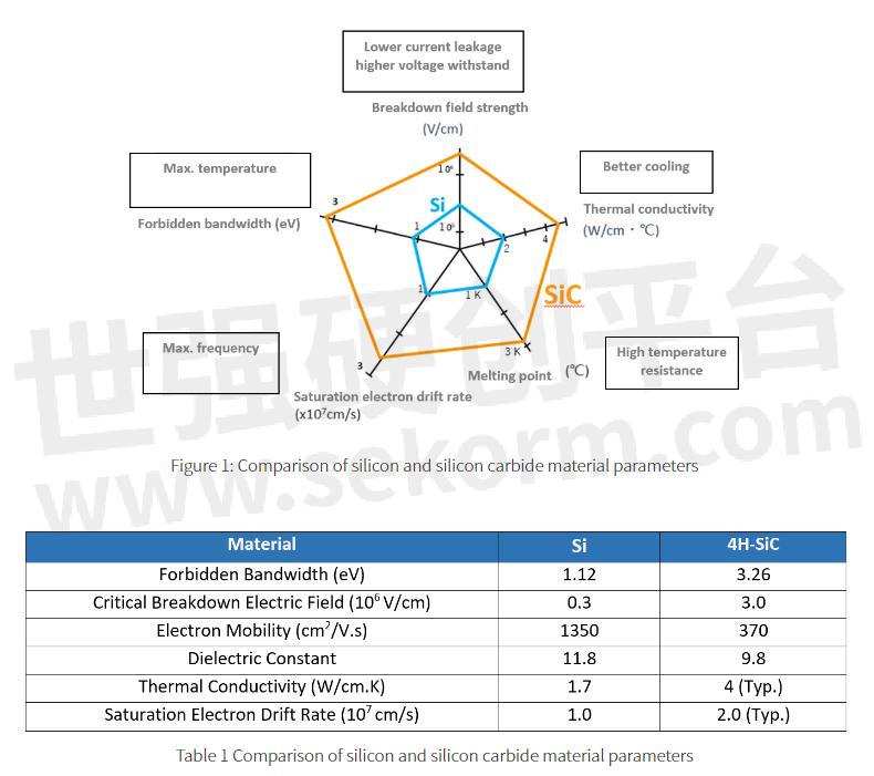
The third-generation semiconductor silicon carbide is currently the hottest topic in the semiconductor field. When it comes to silicon carbide (SiC), the first thing that comes up is its performance advantages, such as lower loss, higher voltage, higher frequency, smaller size, and higher junction temperature, making it ideal for manufacturing high-power electronic devices. In terms of applications, the relatively high cost of SiC makes customers hesitant to choose. In fact, in some applications with performance, efficiency, size, heat dissipation, and even system cost requirements, the cost gap between silicon carbide devices and silicon devices is narrowing. One typical example is the power supply industry.
Since silicon carbide materials have such obvious advantages, what benefits can silicon carbide Schottky devices actually bring?
1. Advantages of the device itself
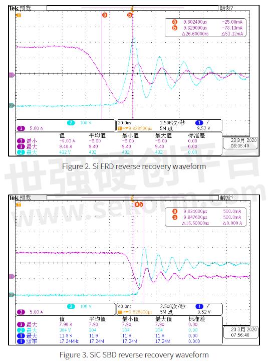
High breakdown voltage (commonly used voltage 650V/1200V), high reliability (junction temperature 175℃ ), small switching losses and conduction losses, device reverse recovery time is almost 0, and the recovery voltage stress is small (refer to the figure below), which helps to reduce system noise and improve EMI margin.
2. Advantages of Application
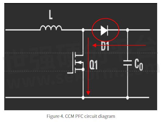
In CCM PFC circuits, the zero reverse recovery current of the silicon carbide Schottky reduces the current stress at the moment the main power MOSFET turns on, allowing it to convert power with less thermal loss. Silicon semiconductors must be much larger to achieve the same performance. This is reflected in the product, namely the silicon carbide Schottky in lower power supply temperature to improve conversion efficiency while also significantly reducing the size of the power supply, which will bring significant benefits to manufacturers.
As an integral part of the power system, power semiconductors are one of the decisive factors in enhancing energy efficiency. In the history of Schottky's development, the pursuit of lower losses has been a common goal of the industry. Schottky device losses are mainly caused by conduction losses and switching losses, and useless power losses are released in the form of heat generation lines, causing an increase in power supply temperature.
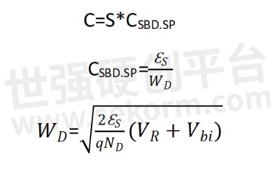
The conduction loss and forward voltage drop are positively correlated. Therefore, according to the VF forward voltage drop equation and the decomposition of the equation, we can conclude that reducing the chip thickness can effectively reduce VF. Thus, reducing the conduction loss.
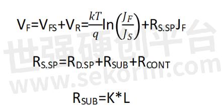
Moreover, the switching loss is positively related to the capacitance value. According to the derived equation, reducing the junction area can effectively reduce the capacitance value and thus the switching loss.
From a designer's perspective, the balance between forward voltage drops and capacitance is critical. The use of new processes can lead to better overall performance. The current process nodes for silicon carbide Schottky products can be broadly divided into the following four:
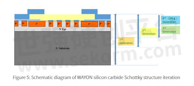
The first generation: chip thickness of 300μm or more for the process node, the common thickness is 300μm, 350μm, and 390μm. This process makes the chip thicker, which requires less scratching, metallization, and other processes in the processing. At the same time, the disadvantage is also obvious, due to the thicker chip, it is difficult to get a better comprehensive performance between the forward voltage drop and capacitance. Only a small number of domestic manufacturers are still using this process.
The second generation: Products are represented by a chip thickness of 250μm. At present, most of the mass production products of domestic manufacturers use this process. WAYON's first-generation products are also developed based on this process (currently updated to the third generation). Yet, compared to the international first-tier manufacturers there are still some gaps in this technology.
The third generation: Products are represented by a chip thickness of 150μm. This process is a new technology platform launched by most domestic manufacturers at the end of 2021 to early 2022, most manufacturers are still in the research and development stage. At the same time, some of the international first-tier manufacturers have adopted 150μm process to mass produce, such as the CREE C6 series. Yet there is still a gap between this process and the international best level.
The fourth generation: Products are represented by 100μm thickness. This process level is the current best mass production level in the world. For example, Infineon C6 and other products are developed using this node process, obtaining the comprehensive advantages of VF and capacitance performance. This node is also used in WAYON's current mass production process, which is 1 to 1.5 generations ahead of the domestic mainstream.
After 3 years of research and development, coupled with continuous self-optimization and iteration during the development process, WAYON's silicon carbide Schottky products have been updated three times: 250μm, 150μm, and 100μm. At present, all mass production products adopt a 100μm node (WAYON's third generation) thin chip process, which reduces capacitance by reducing chip thickness, and conduction loss and using the method of reducing the effective junction area, so that the performance of device parameters such as device current density, conduction loss and switching loss is superior to the level of the industry.
Cell phones and other consumer power supplies, solar inverter power supplies, new energy electric vehicles and charging piles, industrial control special power supplies, etc. As an important and rapidly developing application area, the development of the power supply industry benefits from the technological progress of power devices, which in turn promotes the development and manufacture of power devices. The use of silicon carbide Schottky devices in power supply modules has the following advantages:
·Very low switching losses;
·Higher switching frequencies;
·High junction temperatures, resulting in reduced cooling requirements and heat dissipation requirements;
·Smaller packages for more compact solutions.
Government industrial encouragement policy is important, but the real market demand, better user experience, and product advantages are the keys to triggering the market.
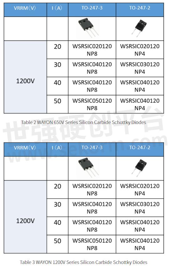
WAYON Silicon Carbide Schottky presents the following series of products:
WAYON continues to work on the development of Silicon Carbide Schottky Diodes with lower losses and higher switching speeds. The products are still undergoing continuous self-optimization, and the fourth generation is under development.
- +1 Like
- Add to Favorites
Recommend
- The Advance of WAYON Domestic IGBT, with higher power cycle life and higher robustness
- Preferred Power Solution: Wayon VDMOS Offers High Versatility and Durability
- WAYON Offers the Bridgeless 240W Power Module Solution with Both High Power and High Energy Efficiency
- Booster in the Field of Adapters -- WAYON Power Schottky Diodes with Voltage Ranges from 45 to 200V
- WAYON Launches AEC-Q100 Automotive Grade 8-bit MCU – WY8A8503
- WAYON‘s 500V-1500V, Current Covering 2A~40A VDMOSFET for More Power Control
- Diverse Specifications, Flexible Packaging: WAYON‘s Thyristors Meet Your Various Needs
- The “Magic Bullet“ for High-Current Scenarios, the Advantages of WAYON TOLL MOSFETs Explained
This document is provided by Sekorm Platform for VIP exclusive service. The copyright is owned by Sekorm. Without authorization, any medias, websites or individual are not allowed to reprint. When authorizing the reprint, the link of www.sekorm.com must be indicated.
Integrated Circuits


Discrete Components


Connectors & Structural Components


Assembly UnitModules & Accessories


Power Supplies & Power Modules


Electronic Materials


Instrumentation & Test Kit


Electrical Tools & Materials


Mechatronics


Processing & Customization


