How Are Semiconductors Made?

Semiconductors enable billions of electronic devices that we use daily, but how exactly are they created?
How Are Semiconductors Manufactured?
Billions of semiconductors enable the electronification of the world around us. What begins as a simple chemical element ends up powering everything from consumer electronics like calculators and mobile phones to advanced computer systems like self-driving cars and in-flight rocket controllers. Semiconductors store data, perform logic functions, and much more. But how do they go from purified silicon to enabling the entire interconnected, electronic world?
Creating Silicon Wafers
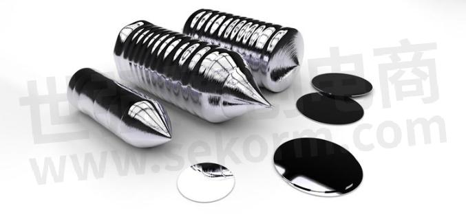
Semiconductor manufacturing begins with a simple element like silicon (often purified from sand or quartz). Once silicon is highly purified, it is shaped into a cylindrical crystalline ingot called a silicon boule. The boule is cut into very thin, uniform wafers with a wide range of different diameters depending on the boule size and required chip yield.
Each wafer is exposed to elements like boron or phosphorus in precise quantities in a process called semiconductor doping. This changes the electric properties of the material and allows semiconductors to accomplish different functions.
The doped silicon wafers are introduced to gases in a thermal processing system. While the specific deposition method may vary, the goal is always to produce an oxide layer on the wafer that protects the silicon surface, as any contaminants could interfere with the electrical current.
Photolithography and Thin Film Deposition
Depending on the use of the integrated circuit (IC), a complex system of integrated components such as transistors, diodes, capacitors, resistors, and more are transferred onto the wafer via photomasking. Once the circuit designs are traced onto the wafer, they are etched into it through wet etching (liquid etchants) or dry etching (plasma etchants).
While semiconductors are incredibly thin, they include dozens of layers of material stacked on top of one another from the photoresists and etching. A thin film of conductive and insulating layers is then added to the circuit pattern. Interconnects are attached to the wafer to electrically connect all the layers together.
Wafer Testing and Semiconductor Dicing
Now that the wafer is complete with the necessary interconnected circuits, it goes through initial testing. Wireless or wired automated test equipment (ATE) performs electronic die sorting (EDS) that includes circuit probing, repair processes, wafer burn-in, and more to identify faulty semiconductor chips along the wafer to remove them from yield once the semiconductor chips are cut out.

Semiconductor chips are finally individually cut from the wafer along predetermined lines via a blade in a process called semiconductor dicing. Depending on what the chip is being used for, it's inserted into semiconductor test sockets to be tested for voltage, current, resistance, capacitance, and more.
Semiconductor Packaging
Passing semiconductors then go through the final stage of semiconductor production: integrated circuit (IC) packaging. The semiconductor chip is attached to bonding wires and encapsulated into a package made of plastic, ceramic, metal, or some combination. The package protects the delicate chip from corrosion, moisture ingress, and physical damage. Thermal and electromechanical solutions such as EMI shielding and heat transfer fins can also be incorporated into the packaging at this step.
Each integrated circuit package also contains an array of leads that are used to connect the IC to a circuit board. These are often made up of pins in a pin grid array (PGA), solder in a ball grid array (BGA), or flat no leads (QFN/DFN) packages depending on size and connectivity requirements. Recently, some IC packages have evolved into system-in package (SiP) constructions, where multiple semiconductor chips are packaged together for a three-dimensional integrated circuit.
Finally, the integrated circuit packages are carefully packaged and sent to the end user, where they may undergo system-level testing to test each chip in the context of where it will ultimately be used.
The Boyd Difference for Semiconductor Solutions
From unique temperature forcing equipment for semiconductor testing to the custom immersion cooling systems that cool processor chips in data centers, Boyd's integrated circuit solutions help cool, seal, and protect nearly every aspect of the semiconductor industry. Boyd's experts blend decades of experience working with leading semiconductor producers with cutting-edge innovation to enable higher processing power in smaller footprints.
- +1 Like
- Add to Favorites
Recommend
- Laird Thermal Systems‘ Next Generation Heat Exchanger LA5000 Economically Provides Full-Time Operation for Immersion Cooling in Data Centers
- Laird Thermal Systems Custom Solutions for Cooling Medical X-ray Imaging Equipment
- Aavid‘s Liquid Cooling Systems: Modular or fully customized liquid cooling optimized for improved heat dissipation in condensed volumes
- Aavid‘s Modular Liquid Cooling Systems: Build a semi-custom system with high performance compatible components
- Laird Thermal Systems‘ Testing Liquid Cooling Systems Can Be Tailored According to Customer Specifications and Applicable Industry Standards
- Laird Thermal Systems’ Prototyping Liquid Cooling Systems
- Laird Thermal Systems’ LA5000 Liquid-to-air-based Heat Exchanger System for Cooling X-ray in Industrial Scanners
- Laird Thermal Systems Provides the Liquid Cooling Options for PET and SPECT Scanners
This document is provided by Sekorm Platform for VIP exclusive service. The copyright is owned by Sekorm. Without authorization, any medias, websites or individual are not allowed to reprint. When authorizing the reprint, the link of www.sekorm.com must be indicated.


