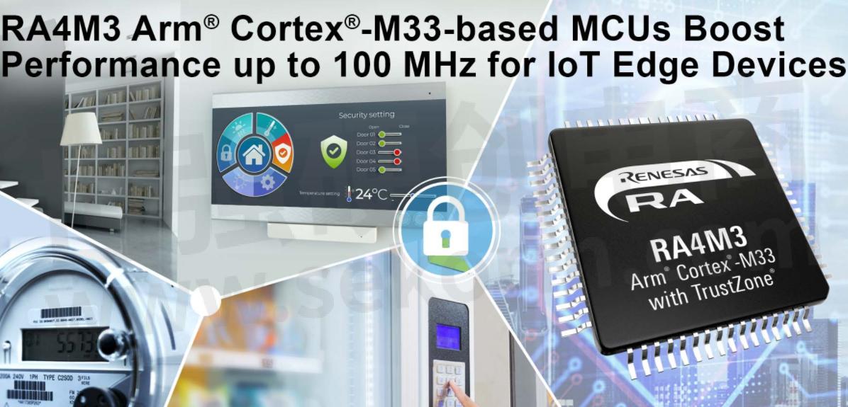
Renesas Extends Arm Cortex-Based MCU Family with RA4M3 MCU Group for Industrial and IoT Applications
TOKYO, Japan ― Renesas Electronics Corporation (TSE:6723), a premier supplier of advanced semiconductor solutions, today expanded its RA4 Series microcontrollers (MCUs) with the new 32-bit RA4M3 Group of MCUs. The RA4M3 MCUs boost operating performance up to 100 MHz using the Arm® Cortex®-M33 core based on Armv8-M architecture. Featuring industry-leading performance, Arm TrustZone® technology, Renesas’ Secure Crypto Engine, and a suite of new memory enhancements, the RA4M3 Group makes it easy to develop safe and secure IoT edge devices for low-power applications, such as security, metering, industrial, and HVAC applications.
“I am excited about the rapid expansion of the Renesas RA MCU family following our RA6M4 MCU Group introduction last October,” said Roger Wendelken, Senior Vice President of Renesas’ IoT and Infrastructure Business Unit. “While RA6M4 target applications demand superior performance and advanced security, the RA4M3 Group offers a well-balanced combination of performance and power consumption with the same advanced security and safety. In addition, customers can take full advantage of the flexibility for memory expansion options that are typical for a broad range of industrial and IoT applications that require continuous innovation.”
The RA4M3 Group is designed for low-power IoT applications that require a balance of high performance, strong security, and higher memory. The RA4M3 MCUs combine TrustZone technology with Renesas’ enhanced Secure Crypto Engine, enabling customers to realize secure element functionality in a wide variety of IoT designs. The Secure Crypto Engine incorporates multiple symmetric and asymmetric cryptography accelerators, advanced key management, security lifecycle management, power analysis resistance, and tamper detection.
The RA4M3 MCUs drive power consumption down to 119uA/MHz in active mode running CoreMark from flash memory and 1.6mA in standby mode with standby wakeup times as fast as 30 µs – a critical element for IoT applications operating in the field for extended periods. For memory-intense applications, designers can combine Quad-SPI and SD-card interfaces with the MCUs’ built-in embedded memory to increase capacity. The background operation and Flash Bank SWAP option is ideal for memory optimized firmware updates running in the background. The increased embedded RAM with parity/ECC also makes the RA4M3 MCUs ideal for safety-critical applications.
The RA4M3 MCUs also feature several integrated features to lower BOM costs, including capacitive touch sensing, embedded flash memory densities up to 1 MB, and analog, communications, and memory peripherals.
Key Features of the RA4M3 Group
100 MHz Arm Cortex-M33 with TrustZone technology on a 40nm process
Integrated 1 MB flash memory, 128 KB RAM, 8 KB Data Flash and 1 KB stand-by SRAM
Low power consumption delivering an operating current of 119 μA/MHz in active mode and 1.6 mA standby current with 30 µs wakeup time
Background operation and Block SWAP function for the flash memory
Capacitive touch sensing unit
Multiple interfaces including Quad SPI and SDHI memory interfaces, SSI, USB2.0 Full Speed, SCI, and SPI/I2C
Scalable from 64-pin to 144-pin LQFP packages (including LGA- and BGA-ready options)
Together, the RA4M3 Group with Flexible Software Package (FSP) allows customers to re-use their legacy code and combine it with software from partners across the vast Arm ecosystem and the RA partner ecosystem to speed implementation of complex connectivity and security functions. The FSP includes FreeRTOS and middleware, offering a premium device-to-cloud option for developers. These out-of-box options can be easily replaced and expanded with any other RTOS or middleware.
The FSP provides a host of efficiency enhancing tools for developing projects targeting the RA4M3 MCUs. The e2 studio Integrated Development Environment provides a familiar development cockpit from which the key steps of project creation, module selection and configuration, code development, code generation, and debugging are all managed. The FSP uses a GUI to simplify the process and dramatically accelerate the development process.
- RA系列NIST SP800-22R1A RA4M3随机数统计测试报告
- RA4M3机组高温作业注意事项
- 用于RA4M3微控制器组的RA4M3组评估套件
- 瑞萨RA系列ARM®DSP示例
- Renesas RA Family:Installing and Updating Secure Keys
- 用于RA4M3微控制器组EK-RA4M3的RA4M3组评估套件
- 用于RA4M3微控制器的RA4M3组评估套件EK-RA4M3快速入门指南
- RA系列IEC 60730/60335 RA MCU自测库(RA4_CM33)
- 用于RA4M3微控制器的RA4M3组评估套件EK-RA4M3 V1勘误表
- 在系统总线上使用S缓存的Renesas RA系列指南
- 基于ARM®Cortex®-M33的RA系列MCU的标准引导固件
- RA4M2组、RA4M3组、RA6M4组、RA6M5组、修正安全加密引擎(SCE9)技术更新(TN-RA*-A0095A/E)
- +1 Like
- Add to Favorites
Recommend
This document is provided by Sekorm Platform for VIP exclusive service. The copyright is owned by Sekorm. Without authorization, any medias, websites or individual are not allowed to reprint. When authorizing the reprint, the link of www.sekorm.com must be indicated.
Integrated Circuits


Discrete Components


Connectors & Structural Components


Assembly UnitModules & Accessories


Power Supplies & Power Modules


Electronic Materials


Instrumentation & Test Kit


Electrical Tools & Materials


Mechatronics


Processing & Customization


