ATP Offers 3D NAND Flash in Various Form Factors With Capacities Ranging From 128 Gb to 1 Tb, Better Than Planar Nand Solutions

3D NAND SSD: Breaking Scaling Limitations of 2D Planar NAND
Flash-based solid state drives (SSDs) have gone a long way since Dr. Fujio Masuoka invented flash memory in the 80s. In succeeding decades, technologists have successfully developed new methods and used new materials to scale down flash memory chips in order to fit more on a die and increase capacity.
Scaling, however, is expected to reach its limit. Manufacturers try to cram more cells to the same die, but we are nearing technological limitations where photolithography could no longer be shrunk further.

The Need for a Radical Shift from 2D
In 2D planar NAND, memory cells are arranged side by side on a single die layer. Drive capacity is determined by how many cells will fit on the die – more cells mean higher capacity. This technology, however, is limited by the following:
Scaling limitations. Manufacturers have been scaling down memory cell sizes in order to fit more in a die. Technological limitations will be reached, and time will come when photolithography could not be shrunk anymore.
Cell-to-cell interference. Continually shrinking the memory cells leads to the leakage or migration of electrical charge from one cell into an adjacent cell. Current 2D NAND lithography is at 1y/1z nm. Going beyond that is extremely difficult because as cells shrink, electron leakage increases. The smaller the die the NAND is built on, it becomes more and more difficult to prevent writes to one cell from corrupting data in other cells. This occurrence, called cell-to-cell program interference, drastically reduces the reliability of the flash memory and eventually leads to data corruption.
Similar to a congested metropolis finding ways to make more effective use of available land, a radical shift is needed to increase density within a limited die size.
Conquering the Limits of 2D
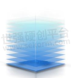
Three-dimensional NAND is the next generation of flash memory technology. 3D NAND breaks through the boundaries of 2D planar NAND by vertically stacking multiple layers of materials, and then a myriad of processes are used to form layers of cells. This innovative technology increases capacity in a given footprint without excessive shrinking of the flash memory chips to fit more on the limited die size. Leading manufacturers are already stacking up higher, ramping up production of 64-layer 3D NAND. Capacity is obviously increased, but there are more benefits. By stacking layers vertically, larger NAND cells may be used, resulting in better performance and endurance. It can be likened to a tall building where you can have many stories or floors within a limited land area. 3D NAND also consumes less power; yields lower cost per gigabyte; generates faster read/write by using simpler algorithms; and delivers better reliability, endurance and overall performance by reducing cell-to-cell program interference.
Summary of 3D NAND Benefits
Better performance and speed. The use of simpler algorithms speeds up read/write performance by 1.3~2x faster.
Lower power consumption. Up to 50% less power is consumed, compared with planar NAND.
Better endurance. 3D NAND reduces cell-to-cell interference, resulting in better reliability and longer SSD life.
Cost efficiency. As 3D NAND becomes more prevalent, it will eventually replace 2D planar NAND, thus driving continued bit cost reduction and paving the way for broader flash adoption in both enterprise and consumer segments. Flash bit cost reduction is expected to decrease significantly via 3D NAND technology.

Table 1. Comparison between 2D and 3D NAND.
The ATP 3D NAND Advantage
ATP offers 3D NAND flash in various form factors with capacities ranging from 128 GB to 1 TB. ATP M.2, 2.5" SSD, mSATA and SlimSATA drives deliver maximum sequential read/write performance of 550/450 MB/s, which is significantly better than planar NAND solutions.
ATP's self-packaging capabilities ensure full control of the production process and quality management from IC level testing to final 3D NAND packaging, assuring customers of shorter lead time, BOM stability and control, customized packaging, and total cost effectiveness.
On top of all these, ATP's self-packaged 3D NAND products also feature advanced technologies to ensure data integrity, durability and trustworthiness even in the most rugged and demanding operating environments.
With 3D NAND evolving fast, it is expected to replace planar NAND in the foreseeable future. Enterprises wanting to meet intensifying data storage needs will benefit greatly from ATP's 3D NAND solutions with their higher capacities, better performance, longer endurance and lower cost per gigabyte.
ATP 3D NAND Solutions
ATP 3D NAND solutions come in different form factors and capacities. Please refer to the table below.
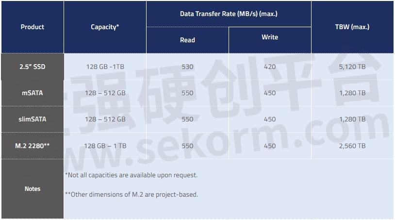
Table 2. ATP 3D NAND solutions.
- +1 Like
- Add to Favorites
Recommend
- SMART’s DuraFlash N200 SATA 2.5” Solid State Drives Provide Economic Yet Highly Reliable Mass Storage
- SMART’s DuraFlash ME2 SATA 2.5” Solid State Drives Offer Highly Reliable Mass Storage with 3D NAND Technology
- SMART’s DuraFlash CS210 SATA 2.5” Solid State Drives are Designed for General-purpose Industrial Applications
- SMART‘s DuraFlash R800 SATA M.2 2280 Solid State Drives,available in both Commercial and Industrial Temperature Ranges
- ATP Customizes PowerProtector Firmware in Solid State Drives(SSDs) for a Leading Aerospace Company
- T5PF 2.5”SATA Solid State Drives With FIPS 140-2 Compliance Deliver High Performance
- T5PFLC 2.5″ and M.2 2280 SATA Solid State Drives (SSDs) Come Equipped with FIPS 140-2 Encryption Capabilities
- What Is a Semi-Solid State Battery?
This document is provided by Sekorm Platform for VIP exclusive service. The copyright is owned by Sekorm. Without authorization, any medias, websites or individual are not allowed to reprint. When authorizing the reprint, the link of www.sekorm.com must be indicated.
Integrated Circuits


Discrete Components


Connectors & Structural Components


Assembly UnitModules & Accessories


Power Supplies & Power Modules


Electronic Materials


Instrumentation & Test Kit


Electrical Tools & Materials


Mechatronics


Processing & Customization


