Recommending the H8S Family Microcontroller IP to Users Looking For H8/3048-like IP

The first Microcontrollers of the H8 family were released in 1988 by Hitachi, Ltd. The architecture was entirely designed and developed in Japan. Renesas took over the manufacturing and sales of H8 microcontrollers in 2003. However, they are now non-promoted products, so Renesas is no longer accepting new orders for H8 series silicon devices. For silicon devices, Renesas recommend an RX microcontroller as an alternative.
However, Renesas still sell H8 microcontroller designs as IP. Renesas has the following families of 8-bit microcontrollers,16-bit microcontrollers, and 32-bit microcontrollers.

The best-known group of microcontrollers among the H8 series is probably the H8/3048F products of the H8/300H family. Devices of the H8/3052F group are also contenders, having almost the same configuration as the H8/3048F except for the flash memory capacity. I found a catalog from 2003, and present part of it as Figure 1.

Figure 1. A roadmap of H8 microcontrollers incorporating flash memory from the catalog in 2003. The H8/3048F group is one of the first-generation product ranges and the devices initially required dual power supplies but were later available as single power-supply versions, H8/3048F-ONE.
In view of this background, it might be assumed that Renesas should promote the H8/3048F IP as the main 16-bit microcontroller product of the family. However, we decided to promote the H8S as the main IP for several reasons.
Firstly, products of the H8S family run at higher speeds than the H8/3048F, yet provide upward compatibility with the H8/3048F. Secondly, at least before the release of H8 microcontrollers with flash memory in1994, the design was not with the use of hardware description languages such as Verilog-HDL. Instead, the design of the H8/3048F took the form of circuit diagrams created with the use of CAD. Figure 2 shows a picture of the CPU part so that you can see its structure.

Figure 2. The CPU portion of a first-generation H8/300H-series product with an instruction decoder at the top, and data path at the bottom.
On the other hand, the H8S series was designed by rewriting the H8/300H circuits in Verilog-HDL and adding some functions. Accordingly, this allows logic synthesis with the use of the EDA tools of today. These are the reasons why Renesas decided to promote the IP for the H8S family instead of that for the popular H8/3048F group.
You may have concerns regarding the use of the H8S instead of an H8/300H microcontroller like aH8/3048F. Renesas has prepared the following information in response to such possible concerns.
1. Aren't there differences between the instruction sets for the H8S and H8/300H?
There is no need for concern on this point because the H8S provides upward compatibility with the H8/300H. While the H8/3048F has 62 instructions, the H8S the H8S/2000 CPU has 65 and the H8S/2600 has 69. There was no decrease in the number of instructions.
2. Aren't there differences between the MCU operating modes?
The two types of products have differences on this point, but you can realize the same configuration as the H8/3048F with the H8S. In the expanded modes (operating modes 1 to 6) of the H8/3048F, the bus mastership is released to an external device, and address spaces in external memory can be used. The H8S IP does not support this functionality because, with the current technology, the user can incorporate any memory into the ASIC design, so external DRAM is not generally required.
Note: Technically, Renesas did support the given functionality in the derived IP. However, the bus was changed to be driven by the selector from the original tri-state-driven bus. This is beyond consideration for implementation on an FPGA.
3. Aren't the flash memory specifications different?
The difference will not be a problem because you can connect flash memory from a new IP rather than using the original one. The original on-chip flash memory of the H8/3048F required the writing of data with a 12-V power supply, which is not required in current designs. Using this old technology in today's chips has no advantages. You can freely add memory as required.
4. Aren't the bus interface specifications different?
As mentioned in (2), the H8S IP does not support an external bus for connection to devices external to the chip. The specification of the internal bus for connection of the internal peripheral modules also differs between H8S and H8/3048F devices. In most cases, however, the new modules are connectable to the bus.
5. Don't the peripheral modules have differences?
The two product ranges do have differences in this respect. In response to such concerns, Renesas prepared the H8S C3000 subsystem IP, in which peripheral modules similar to those of the H8/3048F such as the interrupt controller and timer unit are connected to the H8S core.
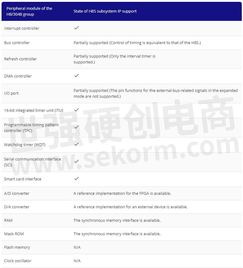
The table below lists the peripheral modules of the H8/3048 group that the H8S subsystem IP supports. Note that the modules supported by the H8S subsystem IP are not exactly the same as those in H8/3048F devices. They are newly revised modules.

For example, in the new modules marked with a check (check) in the table, new functions are allocated to the reserved bits of registers. However, the difference will not create a problem because the modules have been extended, debugged, and the RTL code for each module has been cleaned up.
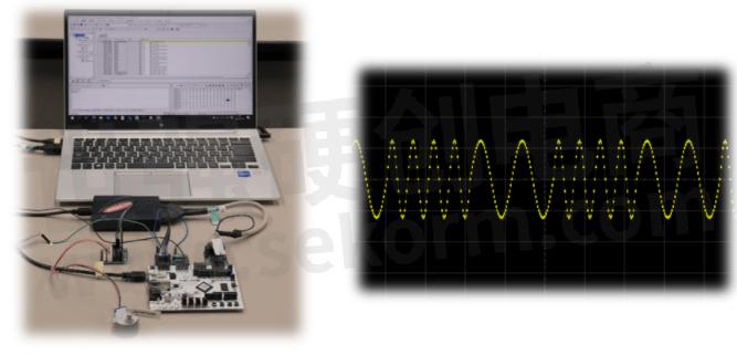
Figure 3 shows an example of the H8S IP implemented in an FPGA, and of the execution of the assembly program described in the H8/300H Series On-Chip Supporting Modules Application Note.

Figure 3. Execution of the assembly program in H8/300H Series On-Chip Supporting Modules Application Note by the IP. On the left is an environment where the 4-phase stepping motor output example is executed. On the right is the result of the sine wave output monitored on an oscilloscope. The external D/A converter is controlled through the registers of the H8/3048F.
As I have explained up to this point, the H8S IP can be used in almost the same way as an H8/3048F device.
Renesas disclose the source code for the IP to customers, so they can modify the settings of the peripheral modules as required. For example, they can change the initial values so that the initial making of settings will not be required.
Renesas strongly recommend using the H8S IP if you are looking for IP for an H8/300H microcontroller such as one from the H8/3048F or H8/3052F group.
- +1 Like
- Add to Favorites
Recommend
- Renesas DSP Solution on Renesas Lab on the Cloud, Input Analog Signals Directly From A Signal Generator To The Rx231 Microcontroller Evaluation Board
- Renesas‘ Semiconductor Manufacturing Factory (Naka Factory) Fire: Production Capacity Has Recovered to 88%
- Renesas Announces 10 New Winning Combinations Integrating Celeno and Renesas Products
- Renesas & Altran to Deploy First Social Distancing Wristwatch Using Ultra-Wideband Chipset with Low Rate Pulse
- Renesas and FAW Establish Joint Laboratory to Accelerate Development of Next-Generation Smart Vehicles
- Renesas Semiconductor Manufacturing Factory (Naka Factory)‘ Production Level Has Returned to 100%
- Renesas and Sequans Expand Their 5G Collaboration including Broadband IoT Module for 5G NR FR1/FR2
- Renesas and Cyberon Partner to Deliver Integrated Voice User Interface Solutions for Renesas RA MCUs Supporting Over 40 Global Languages
This document is provided by Sekorm Platform for VIP exclusive service. The copyright is owned by Sekorm. Without authorization, any medias, websites or individual are not allowed to reprint. When authorizing the reprint, the link of www.sekorm.com must be indicated.


