Renesas Low-Noise Power Supply for Timing and Clock ICs
Renesas offers the broadest and deepest silicon timing portfolio in the industry. In addition to our wide selection of buffers and clock synthesizer products, we deliver leading-edge system timing solutions to resolve timing challenges in virtually any application. With proven expertise spanning more than twenty years in both analog and digital timing, our portfolio features the lowest phase noise and highest performance in advanced timing technology.
The timing and clock ICs are widely used in applications like networking, RF, IoT, telecom, image sensor, medical and even audio applications. When designing the external circuitry around a timing IC, we must pay attention to the power supply design. Just like we should not fill a Lamborghini with cheap gas, we are not supposed to power our low-noise timing ICs with noisy power supplies.
For timing and clock ICs used in all the mentioned applications, the power source is usually either battery or any voltage bus between 5V to AC. The power source voltage is typically stepped-down to an appropriate level through a switch-mode power supply. Here some external radiated or conducted noise may be coupled into the system and the power supply may generate its own internal noise causing its output voltage to carry wide frequency spectrum and inaccurate timing/clock signals to be generated. We should not feed any noise-sensitive timing or clock IC directly from such noisy power supply without adding a strong filter or a low-noise LDO, as shown in figure 1. A low-noise LDO is always preferred over large filters due to size advantage, accurate output voltage and better dynamic load response.
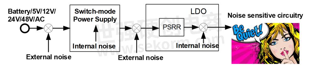
Figure 1 A typical power supply diagram feeding the noise sensitive circuitry
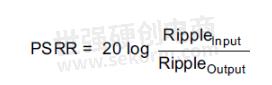
Such low-noise LDO often has very high PSRR (Power Supply Rejection Ratio) to block the incoming noise and it has very low self-generated noise as well. The PSRR is the ratio LDO input voltage ripple vs. output voltage ripple at a specific frequency, and is typically expressed in log form:
The PSRR typically varies with load current, headroom voltage, output capacitor, and, depending on the part, external noise filter capacitor and output voltage. High frequency PSRR can be easily improved by external capacitors. However, for low frequency filtering, the capacitor may become quite large and expensive, therefore selecting an LDO with very high PSRR at low frequencies may help reduce the capacitor size.
Figure 2 shows the PSRR variance over various system settings. Per figure 2B, the PSRR is higher with larger output capacitor at high frequency and the LDO already has very high PSRR at low frequencies. Per figure 2D, if an even higher PSRR at light load is desired, a designer can add a small, low-cost capacitor on the bandgap pin, which improves not only PSRR, but the internal noise as well.
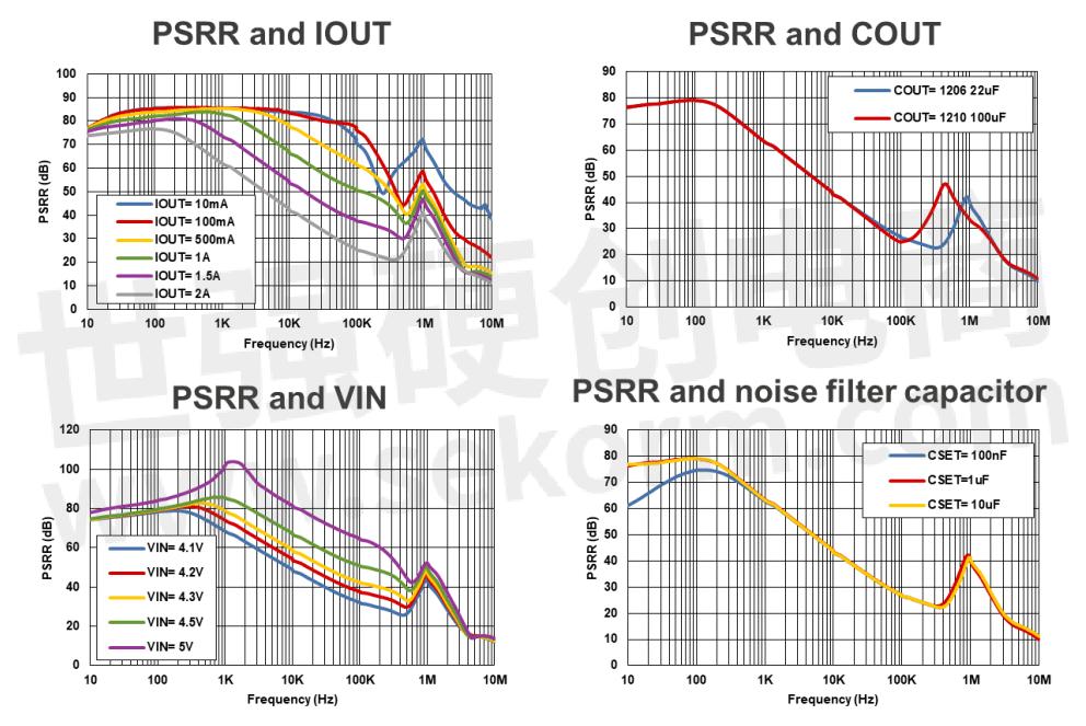
Figure 2 PSRR vs. other system settings
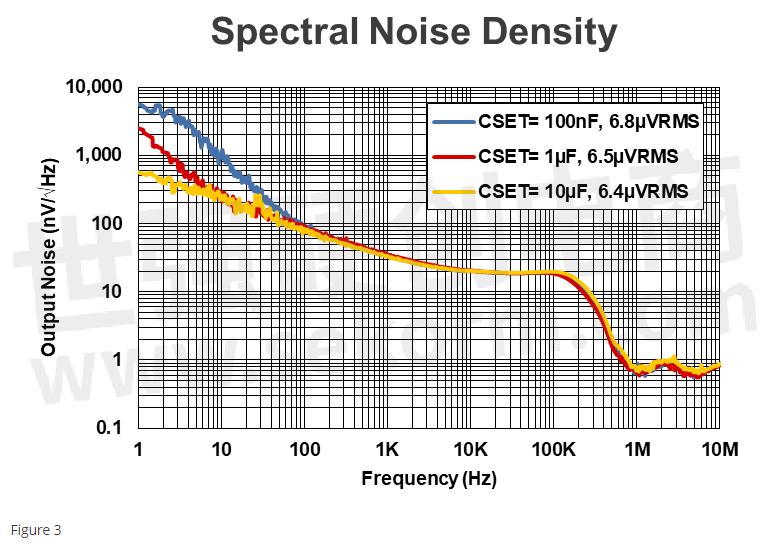
The other important parameter with an LDO is the internal noise, which is indicated in two fashions. One is spectral noise density, a curve that shows noise versus frequency. In applications like RF with regulation on the frequency spectrum, the noise has to be controlled within the “transmit mask” to pass certification testing. Hence, the user should check Spectral Noise Density curves around the frequency of interests. A typical spectral noise chart is shown in figure 3.
The other is integrated output noise, also commonly called output noise voltage. It is the spectral noise density integrated over a certain frequency range. In applications like ADC or DAC, all the LDO noise from DC to the bandwidth of system is integrated and computed as whole to affect the ADC/DAC accuracy. Therefore, total output noise is important for such applications, and a typical chart is shown in figure 4. Figure 3 and 4 are taken from Renesas low noise LDOs with excellent performance.

Renesas has released two ultra-low noise LDOs RAA214020 and RAA214023 rated at 5.5V and 2A output, and they are now fully qualified to power Renesas timing and clock IC portfolio and are included in the BOM of every evaluation board. Some examples are shown below with matching clock IC and LDO devices. More low-noise LDOs of various current rating and performance are coming soon.

In conclusion, for precise timing and clock solutions, customers are encouraged to pair them up with Renesas’ low-noise LDOs to achieve optimized performance.
- +1 Like
- Add to Favorites
Recommend
- Renesas Introduces New ASIL B Power Management IC RAA271082 Ideal for Automotive Camera Applications
- Renesas’ RAA211x Family of Industrial DCDC Regulators Can Reduce the Overall BOM with an Easy-to-use, Scalable Solution
- Renesas Released New High-performance 700V RAA2230xx Regulator Family in Legacy AC/DC Market
- Renesas Provides Automotive Grade PMIC for MCU Power Solution
- Renesas Unveils RAA270205, the First 4x4-channel 76-81GHz Automotive Radar Transceiver with High Accuracy and Low Power Consumption
- Renesas DSP Solution on Renesas Lab on the Cloud, Input Analog Signals Directly From A Signal Generator To The Rx231 Microcontroller Evaluation Board
- Renesas‘ Semiconductor Manufacturing Factory (Naka Factory) Fire: Production Capacity Has Recovered to 88%
- New Highly Integrated Renesas Power Management IC Optimized For RZ/G2L And V2L MPUs
This document is provided by Sekorm Platform for VIP exclusive service. The copyright is owned by Sekorm. Without authorization, any medias, websites or individual are not allowed to reprint. When authorizing the reprint, the link of www.sekorm.com must be indicated.
Integrated Circuits


Discrete Components


Connectors & Structural Components


Assembly UnitModules & Accessories


Power Supplies & Power Modules


Electronic Materials


Instrumentation & Test Kit


Electrical Tools & Materials


Mechatronics


Processing & Customization


