Intellectual Power Amplifier Module Based on GaN FETs

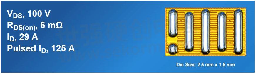
In the past few years, gallium-nitride (GaN) FETs have become more widespread in power electronics. Due to their outstanding characteristics, GaN FETs play an increasingly important role in the miniaturization of the switching converters with very high-power densities exceeding 100 W / cm3 and more. The efficiency of converters based on GaN transistors can reach 99.5%. Due to the extension of the conversion frequency towards the MHz range, the magnetic components (chokes, transformers) also decrease in size significantly. However, designers face numerous challenges in implementing practical GaN transistor designs. The best family members are presented in a wafer-level chip-scale package; the drivers are also quite miniature.
There is a significant problem in optimizing the gate control circuit and its topology due to extremely fast switching speed. As a reminder, GaN FETs have no familiar parasitic body diodes which affect the application design. Taking into consideration the values of the currents and voltages, relative to the size of the power elements, it becomes clear that a new design approach is needed in terms of the PCB topology, heat dissipation, and ensuring the safe area operation for all working modes. As usual, the designer must choose two of three between "Cost", "Efficiency" and "EMC", but for GaN FETs this combination is extended compared to Si MOSFETs.
To simplify and accelerate the development process of many devices (D-class audio amplifiers, AC current and voltage calibrators, power supply modulators, etc.), the idea of creating an Intellectual Power Amplifier Module (IPAM) with the following parameters appeared:
• Supply voltage up to 80 V, output current up to 20 A
• Sinusoidal output power 500 watts
• Efficiency 98% (half power), 96% (rated power)
• Full Power Bandwidth 0…50 kHz
• Main carrier frequency 1 MHz, internal transitions up to 10 MHz
• Less than 0.01% THD (-1dB)
• Diagnostics and parameter setting via 2-Wire Serial Interface (TWI)
IPAM is a fully differential pulsing power amplifier covered by common negative feedback. Typical carrier frequency is approximately 1 MHz and may vary within ±50 % based on the input level, output power, and load impedance. A high-speed precision comparator is used as an error amplifier.
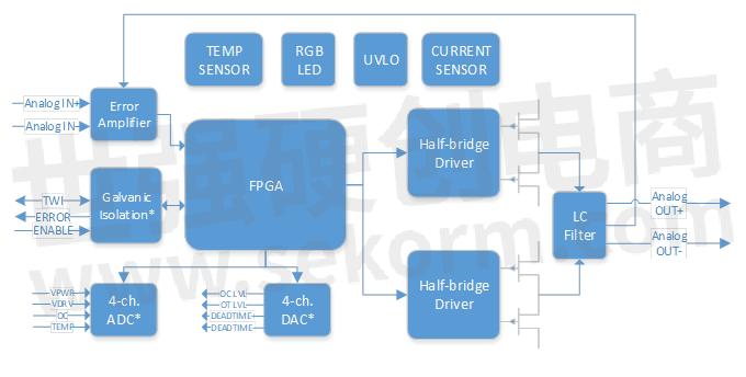
The module contains a small FPGA chip. The first important FPGA function is to produce additional pulses for the best amplifier linearity. The second FPGA function is to maintain safe operating modes of the power switches and the output choke, regardless of the parameters of the input analog or PWM signal. FPGA limits the modulation index and some other parameters. When the transition frequency drops below the limit, the FPGA generates extra pulses that prevent the UVLO detector from triggering due to the discharge of bootstrap capacitors. The minimum pulse length is also limited to comply with the driver circuit possibilities. If the parameters of the input signal corresponding with the introduced restrictions, the pulse sequence from error amplifier output are transmitted asynchronously to the half-bridge drivers, with a delay of fewer than 5 ns and minimal time distortion. All parameters are programmable via TWI and can be deactivated by the user.
IPAM has no dependency on THD+N vs Frequency and has a very low dependency on THD+N vs Output Power thanks to its original control loop structure. For output power up to 200-250 W RMS, IPAM does not require an additional heatsink for generic scenarios.

The problem of heat removal is solved by using a six-layer PCB with 35 µm Cu on the outer layers and 70 µm on the inner layers, and the vias are filled with copper. The module is housed in a CNC-machined aluminum enclosure with 76 x 36 x 18 mm dimensions. At the last stage, vacuum filling is performed with a specialized ceramic-based compound with very high thermal conductivity.
The development of the output choke has turned into a separate R&D work related to the need to study the parameters of the newest high-frequency power ferrites manufactured by TDK/EPCos and Ferroxcube. Unfortunately, these companies did not provide sufficient data for accurate calculations. I had to find a way to make samples with different gaps and different numbers of turns and study them in detail. It took more than one month with the corresponding costs.
As a result, 33 μH small-sized chokes with a 20 A linear current range and SRF > 10 MHz were created. Unfortunately, the world industry does not produce chokes with similar characteristics. I have got about 16 usable chokes with different parameters.
I also had to study the real characteristics of various film capacitors for the output demodulating LC filter and opt for products with a polyphenyl sulfide dielectric. Ceramic capacitors are not suitable for these purposes due to their enormous nonlinearity. Special attention was paid to choose optimal ceramic blocking capacitors for the power stage. I am not sure if I could do this work without Vector Network Analyzer, 2 GHz Oscilloscope with active probes, and a couple of burning experiments at the start. Many reference designs are "thing in itself" and can work only “as is” on your lab table but do not work in a real environment, especially if they are tied up by external connections which produce EMI problems. I managed to achieve that almost all high-frequency components of the switching current circulate inside the module.
Please carefully design the gate driver circuit if you want to achieve high efficiency and do not want to have EMI problems in the future. I highly recommend simulating the circuit by adding parasitic inductances before you start to burn it naturally. With GaN FETs, there is a very thin trade-off between reliable gate control and practical parameters (Efficiency, EMI). It is possible to find a way to keep confident control of the gate. I propose to use several wonderful properties of ferrite beads which can be used for some non-trivial cases. Due to the extremely high dV/dt and dI/dt, significant voltage spikes occur between the power and signal grounds of the module during operation. I added galvanic isolation for TWI and ERR/ENA control signals.
The RGB LED indicates the fact and cause of multiple failures. The types of errors are encoded in series of flashes separated by a long pause. IPAM can be re-initialized automatically, using the built-in timer that generates the protective interval.
A general-purpose 2-phase module without an output demodulating filter is under development. It can be used for a wide range of DC/DC converters with different topologies (buck-, boost- or LLC). A 3-phase version of the power module with similar parameters can be built.
I would like to express my gratitude to EPC European office for the timely support. The result of this big two years’ work is a deep understanding of the capabilities of GaN power electronics. Several architectural, circuitry, topological and design solutions have been developed, which now make it possible to develop a wide range of various devices for breakthrough electronic systems.
- +1 Like
- Add to Favorites
Recommend
- Two Patents Have Been Granted, Further Enhancing Kinghelm‘s Intellectual Property Protection
- CISSOID Announces 3-Phase 1200V/450A SiC MOSFET Intelligent Power Module for E-mobility
- CISSOID Expands Its Sic Intelligent Power Modules Platform for E-Mobility and Aerospace Markets
- CISSOID Will Present Its SiC Intelligent Power Modules & SiC Inverter Reference Design at the 2023 Power Electronics Exhibition
- Modular Power Supply Creates A New Era of Intelligent Power Supply
- CISSOID has Collaborated with NAC Group and Advanced Conversion to Offer 6-Pack DC-Link Capacitors Optimized for CISSOID‘s SiC Intelligent Power Modules
- FORESEE Industrial SSD Products Employ Wide Temperature Technology to Boost Intelligent Industrial Scenarios
- Sharge Selects GaN FETs EPC2218 from EPC for High-power USB PD Charger Retro 67 to Achieve the Most Efficient Power Conversion
This document is provided by Sekorm Platform for VIP exclusive service. The copyright is owned by Sekorm. Without authorization, any medias, websites or individual are not allowed to reprint. When authorizing the reprint, the link of www.sekorm.com must be indicated.
Integrated Circuits


Discrete Components


Connectors & Structural Components


Assembly UnitModules & Accessories


Power Supplies & Power Modules


Electronic Materials


Instrumentation & Test Kit


Electrical Tools & Materials


Mechatronics


Processing & Customization


