the concept of detecting wire bond deformations of an IC using Keysight VTEP technology
My previous post on Detecting Near Short Defects in IC Wire Bonds with VTEP technology shares the concept of detecting wire bond deformations of an IC using Keysight VTEP technology.
The technique depends on the amount of capacitive coupling between the wire bond and the VTEP sensor plate. The aim is to only pick up the capacitive coupling signals from the wire bond area of the IC and minimize the coupling signal strength from other surrounding elements like the lead frames and the die chip itself. To do this, we cut the VTEP sensor plate such that it only covers up to the area where the wire bonds are located.

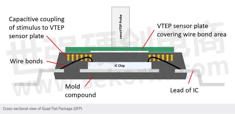
Wire bonding methods in different IC package types limit the effectiveness of this solution. For example, a quad flat package (QFP) arranges all the pins around the perimeter of the device. We can easily modify the VTEP sensor plate to a size that provides the best coverage over the wire bonds and stay clear of the lead frames. There are different packaging methods available for ICT but not all work well with this test solution.
Technology advancements increase the complexity and pin count of an IC which leads to the simple QFP package IC increasing its size significantly to accommodate more pins around its perimeter. However, there is a limit on how big an IC can be before it becomes nonfeasible for production or usage.
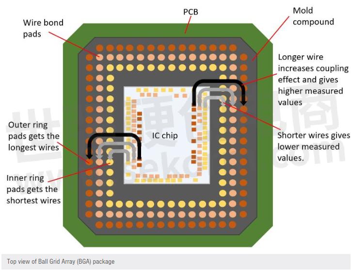
Ball Grid Array (BGA) packaging introduces a new method to handle the increasing pin counts. BGA architecture is different from QFP. Its physical pads are located at the bottom of the IC. The pads route through the printed circuit board(PCB) to the top surface where wire bonds connect them to the IC chip in the middle.
BGA package arranges its wire bond pads in concentric rings around the chip and on the PCB. Pads on the innermost ring of the PCB are the closest to the outermost ring of the chip. On the other hand, pads on the outermost ring of the PCB are the furthest from the innermost ring of the chip. To facilitate the wire bonding process, wiring begins with the shortest wires at the inner ring of the PCB and ends with the longest wires at the outer ring of the PCB.
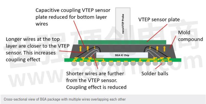
The BGA ends up with the shortest wires right at the bottommost layer and the longest wires at the top. This creates a challenge for VTEP measurement as the wires at the bottom layer are shorter and further away from the VTEP sensor plate above. Multiple layers of wires above the lower wires block the coupling strength and affect its signal-to-noise ratio significantly. This degrades the overall measurement and makes it difficult to achieve the same sensitivity as the QFP design.
The effectiveness of the capacitive wire bond test depends heavily on the wire bonds arrangement of the IC package. Traditional packaging types like QFP and other similar types which have a single layer of wires arranged around the chip provide the best results for the test. This measurement method may also work for simple BGA packages if the wires do not overlap one another.
Therefore, when considering the effectiveness of the wire bond capacitive test solution, remember that it is all about the wire bonds arrangements, rather than the type of IC packaging.
- +1 Like
- Add to Favorites
Recommend
This document is provided by Sekorm Platform for VIP exclusive service. The copyright is owned by Sekorm. Without authorization, any medias, websites or individual are not allowed to reprint. When authorizing the reprint, the link of www.sekorm.com must be indicated.
Integrated Circuits


Discrete Components


Connectors & Structural Components


Assembly UnitModules & Accessories


Power Supplies & Power Modules


Electronic Materials


Instrumentation & Test Kit


Electrical Tools & Materials


Mechatronics


Processing & Customization


