FEA Simulation Aids Signal Integrity in High-Speed Connector Designs

The rapid development of high-speed signal software and hardware across all industries has created a higher level of frequency and bandwidth. Accordingly, the overall performance requirements for connector components are also more stringent. At the same time, the miniaturization of device and package forms interconnects, and other devices within a system present additional design challenges. All these facts have a significant impact on signal transmission integrity.
The basic theory of signal integrity of High-Speed Connectors
As the overall structure of most devices and equipment becomes significantly smaller and operates at higher frequencies, signal integrity issues are arising and require special attention. Characteristic impedance, insertion loss, return loss, and crosstalk — among which impedance and crosstalk have the greatest impact on the signal integrity of a connector — must all be monitored at the testing level to ensure optimal device performance.
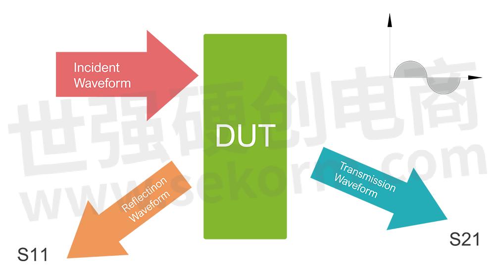
Scattering parameters (S-parameters) are often used in signal integrity as a standard format to describe the broadband high-frequency behavior of interconnects. S-parameters are a format for describing how a standard waveform of an interconnect or component scatters away during the DUT (Device Under Test) process.

Image1: Standard Waveform Input DUT Scattering. In this graphic, Transmission Waveform S21 represents the insertion loss, while Reflection Waveform S11 represents the return loss.
The key factors affecting the signal integrity of high-speed connectors
Generally, the main factors affecting the signal integrity of high-speed connectors are design space, transmission rate, and signal loss. Different PCB layout designs are closely related to these factors, which have a critical impact on the overall signal integrity. Under different PCB layout designs, the high-frequency characteristics presented by the connector will be affected.
At present, the standard high-speed connector has a complete structure and specification to follow. Engineers only need to adjust the design under this structure to meet the high-frequency conditions required by a certain specification. Under normal circumstances, customers can only provide design space and the required transmission rate. In many cases, even the requirements for signal loss are uncertain, which requires different PCB layouts and further adjustments within the design. This is where customized products might be required. Customization in the development of high-speed connectors ensures a high level of signal integrity. Engineers often rely on FEA (finite element analysis) simulation to assist in the design of high-speed connectors.

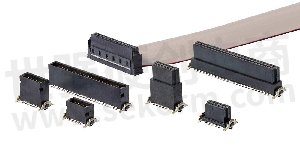
Image2: GREENCONN’s 1.27mm High-speed BTB/WTB Connectors are designed with double-contact spring terminals and have a high signal transmission speed of up to 4GBits.
How FEA simulation assists high-speed connector design
In the customized development of high-speed connectors, Greenconn frequently adjusts the mechanism design to meet customer needs through stress and high-frequency FEA simulation and finally compares the high-frequency characteristics of the product after the process to confirm the validity of the simulation. Multiple comparisons are made to accumulate experience and continuously improve the accuracy of the simulation. The process is divided into the following steps:
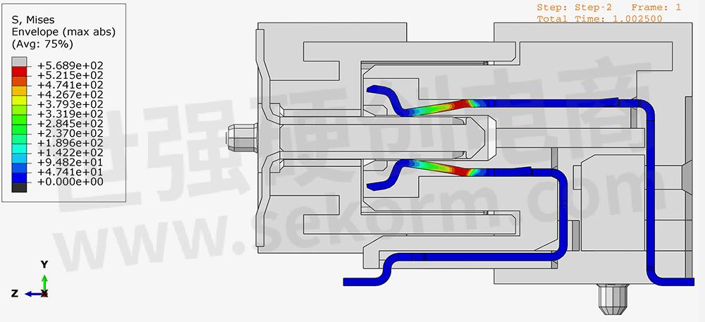
1. After the FEA insertion and extraction simulation, the connector's insertion and extraction force data can be obtained, to judge whether the mechanism design meets the requirements. Furthermore, the deformation state of the terminal can be derived from the simulation results of FEA after the connector is inserted. After multiple verification simulations, as long as the material parameters and FEA simulation conditions are set correctly, the insertion force and state of deformation of the terminals accurately provide results very close to the actual values.

Image3: Greenconn obtains near-actual insertion force data and the state of terminal strain through multiple high-speed connector FEA
2.Add the terminal deformation state found by the FEA simulation and redraw the 3D model of the PCB. Import the drawn model into the high-frequency FEA software and set the parameters of the model to perform the high-frequency simulation.
3. After the continuous and repeated adjustment of design and simulation, S-parameters that meet the needs of customers can be obtained. The four high-frequency conditions are characteristic impedance, insertion loss, return loss, and near-end and far-end crosstalk (NEXT and FEXT).
The signal integrity problems that arise with higher transmission frequencies and the design challenges for the connector become even more severe. In theory, with regard to high-frequency transmission, the more matched the characteristic impedance, the less occurrence of signal integrity problems. However, under the limitation of the space mechanism, the shape of the connector’s contact terminal will be more irregular, resulting from the connector being matched to the high-frequency transmission. Characteristic impedance is difficult, especially as the design of PCB layout has a great impact on signal integrity. Therefore, in the development of customized high-speed connectors, a more accurate reference can be obtained by means of FEA simulation to ensure signal integrity, meet the high-speed transmission requirements required by the equipment, and effectively avoid the waste of resources which therefore results in cost savings.
- +1 Like
- Add to Favorites
Recommend
- The Rise of AI and Its Impact on High-Speed Connector Development in China
- Troubleshooting and Maintenance in High-Speed Connector Applications
- Nextron‘s Next-Gen High-Speed Connectors
- 16 Gbps Colibri High-Speed Connectors with a 0.5-mm Pitch Suitable For Sophisticated High-speed Transmission Applications
- High-Speed Fusing Chip Fuses Play A Crucial Role in Protecting Electronic Circuits
- ept Introduced Colibri 25+ Gbps High-Speed Connectors: Sample and S-parameters Access at Embedded World 2024
- Smiths Interconnect DaVinci 112 Test Socket: A Game-Changer in High-Speed Chip Testing
- Smiths Interconnect’s DaVinci 112 High-Speed Test Socket Wins Best Test Measurement Award at the 2024 Global Electronics Achievement Awards
This document is provided by Sekorm Platform for VIP exclusive service. The copyright is owned by Sekorm. Without authorization, any medias, websites or individual are not allowed to reprint. When authorizing the reprint, the link of www.sekorm.com must be indicated.


