EPC2152 ePower™ Stage – Redefining Power Conversion

Beyond just performance and cost improvement, the most significant opportunity for GaN technology to impact the power conversion market comes from its intrinsic ability to integrate multiple devices on the same substrate. GaN technology, as opposed to standard silicon IC technology, allows designers to implement monolithic power systems on a single chip in a more straightforward and cost-effective way.
Today, the most common building block used in power conversion is the half bridge. In 2014, EPC introduced a family of integrated half-bridge devices which became the starting point for the journey towards a power system-on-a-chip. This trend was expanded with the introduction of the EPC2107 and EPC2108, which integrated half bridges with integrated synchronous bootstrap. In 2018 EPC further continued the integration path with the introduction of eGaN ICs combining gate drivers with high-frequency GaN FETs in a single chip for improved efficiency, reduced size, and lower cost. Now, the ePower™ Stage IC family redefines power conversion by integrating all functions in a single GaN-on-Si integrated circuit at higher voltages and higher frequency levels beyond the reach of silicon.
EPC2152 – 80 V, 12.5 A ePower™ Stage
The EPC2152 is a single-chip driver plus eGaN® FET half-bridge power stage using EPC’s proprietary GaN IC technology. Input logic interface, level shifting, bootstrap charging and gate drive buffer circuits along with eGaN output FETs configured as a half-bridge are integrated within a monolithic chip. This results in a chip-scale LGA form factor device that measures only 3.9 mm × 2.6 mm × 0.8 mm for an 80 V, 12.5 A gallium-nitride based power stage integrated circuit. Depending on operating conditions, the device can operate with PWM frequency range up to 3 MHz, significantly higher than can be achieved with MOSFET discrete or IC solutions.
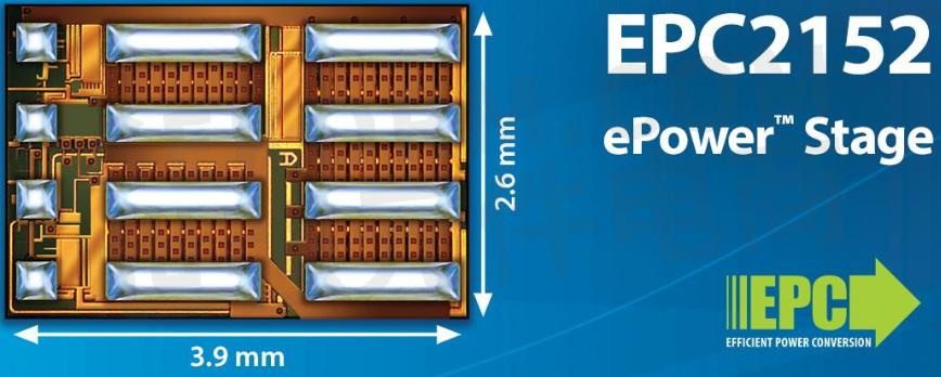
The output devices are configured as a half bridge with RDS(on) less than 10 mΩ for both high-side and low-side FETs. The internal gate drive circuit is designed to match the output FETs and switching time is less than 1 ns from 0 V to 60 V at rated current.
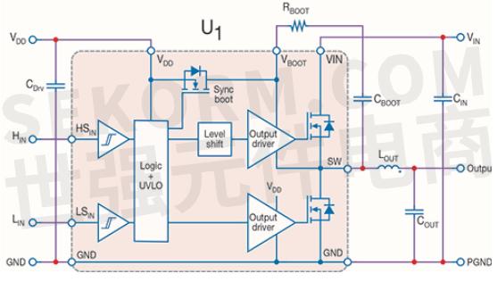
High frequency operation is possible with delay times less than 20 ns and matched high-side vs low-side delay times to ease the use of low dead time less than 10 ns.
Inputs are compatible with 3.3 V logic allowing users to interface directly with MCU or with analog controllers.
The EPC2152 is packaged using a wafer-level chip-scale package (WLCSP) in an LGA outline. The layout of the solder bumps is designed with current flow direction in mind to minimize the power loop inductance in practical PCB applications. EPC’s development board (EPC90120) has a power loop inductance less than 0.2nH.
Ease of Design
The EPC2152 replaces at least three discrete chips; the gate driver plus two FETs making design and manufacturing easier. The device saves at least 33% of space on the printed circuit board compared to a discrete implementation. This family of products makes it easy for designers to take advantage of the significant performance improvements made possible with GaN technology. Integrated devices in a single chip are easier to design, easier to layout, easier to assemble, save space on the PCB, and increase efficiency.
48 V DC-DC
The EPC2152 is targeted to be used for DC-DC converters requiring high efficiency and small size. These are critical benefits for telecom, server and client computing, industrial, automotive and military markets. The device can be designed for buck and boost converters as well as in LLC converters. Some customers are even trying the device in switched cap topology.
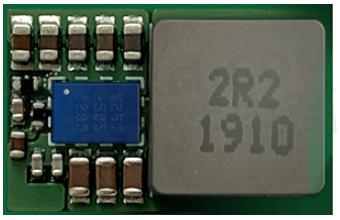
EPC built and tested a buck converter with VIN = 48 V, VOUT = 12 V, fSW = 1 MHz and IOUT = 12.5 A using the EPC2152. The peak efficiency reached above 96% when operating in this buck converter, better than discrete GaN FETs and substantially better than discrete MOSFET or monolithic MOSFET IC-based Power Stage.
Motor Drive
Another promising application for the ePower Stage is motor drive inverters for robotics, drones, and e-scooters. These motor drive applications require a lighter weight, higher bandwidth and lower torque ripple, which are advantages for inverters built using the EPC2152.
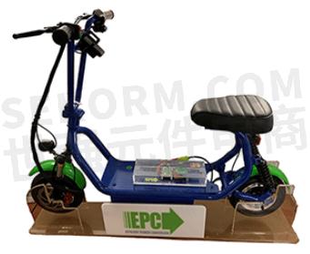
EPC built a prototype using the EPC2152 to power the motor of an e-scooter. The ePower Stage device is employed in a 3-phase sinusoidal excitation, 10 ARMS per phase, 15 A peak motor drive for an efficient, quiet, high performance, and low-cost solution to BLDC motors for e-mobility.
What’s Next
The EPC2152 is the first offering in what will be a wide-range family of integrated power stages available in chip scale package as well as co-packaged modules. Within a year the family will fill out with products capable of operating at high frequency up to 3 to 5 MHz range as well as high current from 15 A to 30 A per power stage.
The ultimate goal is to achieve a single component IC that merely requires a simple digital input from a microcontroller and produces a power output that drives a load efficiently, reliably under all conditions, in the smallest space possible, and economically.
- EPC2108产品/工艺变更通知(PCN)(PCN230301)
- EPC90120开发板快速入门指南
- EPC90120开发板快速入门指南
- EPC90120 80 V半桥,带栅极驱动,使用EPC2152快速入门指南
- EPC90120开发板快速入门指南
- 【Datasheet】EPC2152 80 V, 12.5 A ePower™ Stage data sheet
- 成长中的氮化镓FET功率转换生态系统
- 成长中的氮化镓FET功率转换生态系统
- 【Datasheet】EPC2152x – 70 V, 12.5 A ePower™ Stage
- 【Datasheet】EPC2152x – 70 V, 12.5 A ePower™ Stage
- EPC氮化镓晶体管鉴定报告EPC2107
- EPC氮化镓晶体管鉴定报告EPC2108
- +1 Like
- Add to Favorites
Recommend
This document is provided by Sekorm Platform for VIP exclusive service. The copyright is owned by Sekorm. Without authorization, any medias, websites or individual are not allowed to reprint. When authorizing the reprint, the link of www.sekorm.com must be indicated.


