Microchips Are Manufactured Using Polysilicon and Specialty Chemicals Made by WACKER

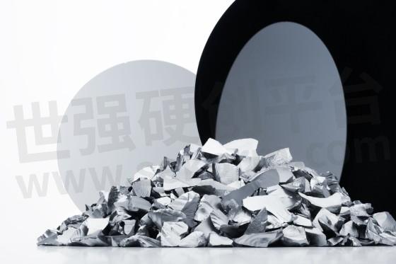
Without polycrystalline silicon, digitalization would be unthinkable. Glossy and silvery in appearance, Polysilicon is among the purest man-made materials and the most important raw material required in the semiconductor industry. Today, nearly one in two microchips are manufactured using polysilicon made by WACKER. And by no means is this WACKER’s only contribution to the industry. Apart from polysilicon, process chemicals by WACKER also play a key role – and the demands on purity and quality are high.
Purity Is Everything
Several hundred steps are required for transforming a silicon wafer to a ready-to-use microchip. Production can take many months and involves extremely challenging technical processes and highly complex equipment. Clearly, constructing a microchip production facility is a costly affair. To be certain their investments pay off, manufacturers must put in every effort to achieve as high a production volume of operational microchips as possible.
That’s not all. Things are made tougher as proper functioning of the semiconductor components can only be verified at the end of the production process. It is therefore no wonder that the microchip industry places the highest demands on the quality of the raw materials and process chemicals supplied and closely monitors the reliability of its suppliers.
Nearly One in Two Microchips Are Manufactured Using Polysilicon Made by WACKER
Microchip manufacturing begins with hyperpure silicon wafers. In almost every case, polycrystalline silicon, or polysilicon, is the raw material required for making these wafers. WACKER is the only semiconductor-grade polysilicon manufacturer in Europe. In fact, WACKER is a global leader when it comes to quantity, quality and material purity. Nearly one in two microchips are manufactured using polysilicon made by WACKER.
Not many though are aware that, in addition to hyperpure polysilicon, WACKER also produces specialty chemicals that are vital in manufacturing computer chips. WACKER silanes, for instance, are used for dispersing and depositing silicon or insulation layers on the wafer surface. Pyrogenic silica from WACKER is used for polishing and leveling the applied layers. And when it comes to cleaning the metalizing chambers, hydrogen chloride, yet another WACKER product, is indispensable.
All electronic chemicals from WACKER are precisely customized to the processes and requirements of the semiconductor industry. Statistical process controls are implemented to continuously monitor the production of these chemicals. After all, the purity of the products must always lie within a very narrow tolerance range that is specified in consultation with the microchip manufacturer. A stringent risk management process is essential, too, to ensure that the product quality is always consistent, even if there are deviations in specific process parameters during production, such as temperature or pressure, or in the event of changes in the production lines.
The majority of the upstream products required for such chemicals are manufactured by WACKER. This makes us less dependent on external suppliers. What’s more, our in-house analytical experts are in a position to precisely detect and quantify even the minutest traces of impurities.
Functional Chemicals and Their Areas of Application
Chemical Vapor Deposition
Process Chamber Cleaning
Chemical-Mechanical Polishing
Silanes for Tomorrow’s Microchips
Every new generation of digital devices tends to display higher switching frequencies and smaller components. Without increasing in size, such devices become faster and more efficient. This is possible thanks to advances involving the miniaturization of the components that constitute a chip.
At the same time, this development becomes more complicated as we move on to the next generation. Today’s microchips have more than one hundred layers superimposed on each other. Design rules of five nanometers – ten thousand times thinner than a human hair – are already standard practice. Such minute dimensions are gradually pushing microchip manufacturers to the limits of what is physically possible.
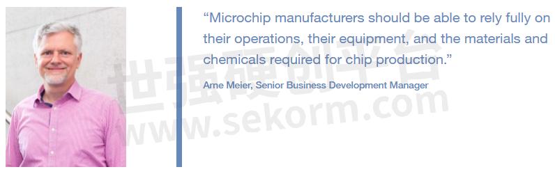
Things get tougher when, for instance, interconnects on a microchip and the insulating layers continue to be packed more closely than ever. High switching frequencies lead to an intensive acceleration of the electric charges in the interconnects whereby relatively strong electric fields are built up. “In the area between the interconnects, the electric fields interfere with each other and thus slow down the charges,” Arne Meier explains. The thinner the insulating layer and the higher the frequency, the greater the slowdown. In extreme cases, the charges do not reach their intended destination in time and the chip fails.
Insulating materials with a lower dielectric constant, represented as “k” in the semiconductor industry, offer a viable solution. WACKER is committed to developing silanes that allow materials with particularly low dielectric constants to be deposited. These silanes can play a key role in tomorrow’s semiconductor industry. According to Arne Meier, WACKER is in the final stages of developing such ultra-low-k materials. “These silanes will be WACKER’s contribution in making the latest generation of computer chips reality.”
Microchips
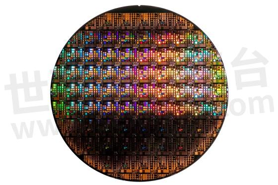
A microchip is an electronic semiconductor component that contains a fully integrated electrical circuit consisting of thousands to billions of tiny transistors, capacitors, resistors and other electronic components. All these elements are arranged in several levels on a semiconductor wafer as microscopically small structures in the form of thin layers that are firmly anchored on the substrate.
Each layer has a function: for example, it can take on the role of an interconnect, be a component of a transistor or act as a resistor. As we move on from generation to generation, we observe a greater miniaturization of the components and, at the same time, an increase in the number of superimposed layers and consequently the number of transistors. A greater number of transistors is what creates a more powerful chip.
Polysilicon is the most important material required to begin wafer production. In this regard, material purity is absolutely crucial. Foreign atoms such as boron or phosphorus are a source of impurities in the semiconductor material and could impact the electrical properties of the semiconductor. This would ultimately lead to the failure of the chips produced from the wafers. The entire focus is therefore on maximum purity.
WACKER’s polysilicon for semiconductor applications has a purity of 12N. This refers to a material that contains no more than one critical foreign atom per trillion silicon atoms, which corresponds to a purity of 99.9999999999 percent. This makes WACKER’s polysilicon the purest man-made material.
WACKER supplies hyperpure silicon in the form of irregularly shaped chip-size material to wafer manufacturers, who produce large cylindrical single crystals from the polycrystalline material and saw them into thin discs that are later planarized, cleaned and polished. The discs are thus transformed into wafers, i.e. the substrates on which the circuit components are mounted. Depending on the chip design and size of the silicon wafer, hundreds of chips are often created from a single wafer. Initially, these chips are laid out next to each other on the wafer like postage stamps and are only separated after the configuration is complete.
- +1 Like
- Add to Favorites
Recommend
- Silicon Labs Simplifies IoT Development with Simplicity Studio 5
- News | Silicon Labs and Amazon Collaborate on Sidewalk, a New Shared Network for IoT Consumer Devices
- Silicon Labs Z-Wave Wireless Selected for Johnson Controls Next Generation Qolsys Smart Home Panel
- Silicon Labs Expands Isolated Gate Driver Product Family Ideal for Hybrid and Electric Vehicles (EV)
- Silicon Labs Strengthens Isolated Gate Driver Portfolio
- Software Speeds Development of IEEE 1588 System Integration | Silicon Labs
- Introducing Silicon Labs’ New Z-Wave 800 Dev Kit for Easy Smart Home IoT Application Development
- Arduino style millis and basic example “Blink without delays“ with Silicon Laboratories Sleep Timer
This document is provided by Sekorm Platform for VIP exclusive service. The copyright is owned by Sekorm. Without authorization, any medias, websites or individual are not allowed to reprint. When authorizing the reprint, the link of www.sekorm.com must be indicated.
Integrated Circuits


Discrete Components


Connectors & Structural Components


Assembly UnitModules & Accessories


Power Supplies & Power Modules


Electronic Materials


Instrumentation & Test Kit


Electrical Tools & Materials


Mechatronics


Processing & Customization


