A Paradigm Shift in Simulation Techniques of Semiconductor Test Sockets
With the rise of the Internet of Everything (IoT), 5G, artificialin tellig ence ( AI ) and augmented reality (AR), high-performance test socket technology must keep pace. Performance specifications for test sockets published by suppliers should only be used as a general guideline in selecting the product family for a test application. Once a socket technology is chosen based on the general specification, suppliers should provide a more representative simulation of the socket based on the customer’s package layout with a focus on the high-speed areas of the device. Typically, simulations focus on the socket in a vacuum and do not consider other features such as the printed circuit board (PCB) pad, vias or the ball grid array (BGA) ball. As data rates and bandwidth continue to increase, a paradigm shift is emerging in the industry that is driving socket suppliers to provide more detailed simulations, which include the device package and PCB interfaces in the analysis because of their impact on final socket performance in the system. Most socket suppliers publish socket characterization data based on an optimum signal/return pin layout (e.g., signal with surrounding returns) as shown in Figure 1. Socket test and characterization are usually done in the design validation stage of development with test coupons that represent the pin and socket structure, but do not include any of the parasitic effects caused by the PCB and package alignment features of the socket.
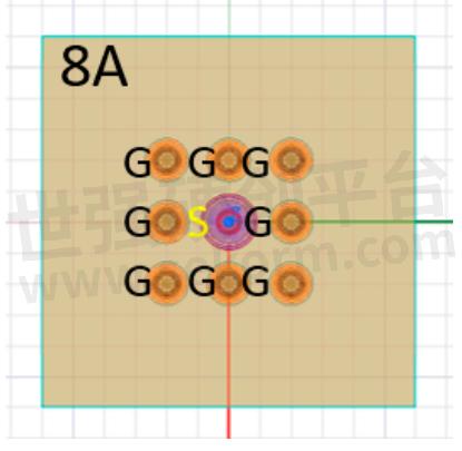
Figure 1: Example of an optimum signal/return pin layout.
The measurement produces S parameters of the entire test setup (Fixture A – device under test [DUT] – Fixture B). The test socket is then de-embedded and gated in order to provide basic performance data, such as the -1dB insertion loss (IL), -10dB return loss (RL), loop inductance (L), and mutual capacitance (Cm) IL, without the effects of test fixtures and/or PCBs. Signal integrity performance data shown in the product collateral regarding the test sockets and contacts usually comes from measurements using this methodology. This information can then be used by the customer to understand the basic performance of the socket and pin in an ideal condition in order to help identify which socket family to use for a given application. Once the buyer chooses the socket technology based on initial performance, they can move into the next phase, which requires a detailed pin-out map of their device for simulation and mechanical socket design. The pin-out map provides a detailed layout of the signal, return and power pins as shown in Figure 2, which will later determine the worst-case radio frequency (RF) performance of the socket that can be expected. As the signal/return pattern changes in the socket, the standard specification data that pertains to the RF performance is no longer relevant as the bandwidth changes, depending on the return layout of the customer’s device.

Figure 2: Example of a pin-out map.
It is good practice to design symmetrical return paths around the high-speed lanes of the customer device so the PCB and test socket can be designed to provide impedance-controlled differential pairs and guard neighboring lanes against cross talk, but real estate constraints don’t always allow chip designers to follow these design rules. Socket designers turn to simulation tools such as HFSS to determine the performance of these complex layouts because it is hardly feasible to measure every instance of a customer’s layout due to package to package variability. It is equally important that these simulation tools are calibrated through correlation to measured data to ensure there is confidence in the result that drives the final decision. Suppliers traditionally ignored BGA and PCB pad during simulation because they do not have control over the design of those features.
Once the layout is established, and the simulation completed, the IL, RL and any cross talk effects are plotted and used to determine if the design is suitable for the application. In some cases, the S-parameter files are provided to the customer for Spice simulation at the system level, but even at this level of analysis, they do not capture the complete system performance due to the parasitic effects caused by the BGA and PCB pad and via. As we shift our focus from simulating test socket performance in a vacuum to include the parasitic effects that PCB pads and the device present to the socket, customers will need to provide these details, along with the pin-out map, in partnering with socket suppliers in the development of the socket technology in order to achieve the best possible system performance. When the socket designer develops a customer solution, a design standard is created to define the mechanical attributes of the socket family that are critical for the customer’s package. Customers are beginning to provide simulation standards that dictate PCB copper thickness, pad diameter, via diameter and length, dielectric constants and loss tangents, and target impedance for the design. It is critical that socket impedance is matched as closely as possible to the PCB impedance to ensure good signal transfer. The target impedance from customer to customer does not always follow the traditional 50Ω or 100Ω standard that is assumed in the absence of such information. The socket designer can then focus on optimizing the interfaces and tuning the socket design to account for these effects. This also assures the customer that simulations are done to their standard and there is consistency from one SI engineer to another. We developed a physical test sample to include a PCB with a short via to interface with the bottom of the socket
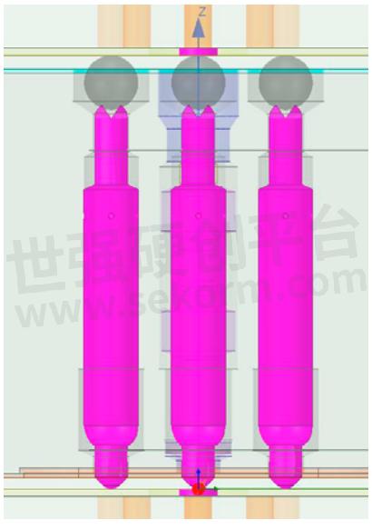
Figure 3: Example of a new simulation set-up used to validate measurements.
and BGA spheres, and a PCB with a short via transition on the top and simulated the same structure to validate the model. An example of the new simulation set-up used to validate the measurement is shown in Figure 3. The simulation and measured results match very well as shown in the single-ended TDR plot in Figure 4. The original TDR measurement without the PCB and BGA used in our standard characterization method to produce the specification data is shown in Figure 5. When comparing the two TDRs, it is obvious that the PCB and BGA create many impedance discontinuities on the signal transmission, which impacts the overall performance. When the socket designer sees the whole stack, the physical design can be optimized to account for these transition points.
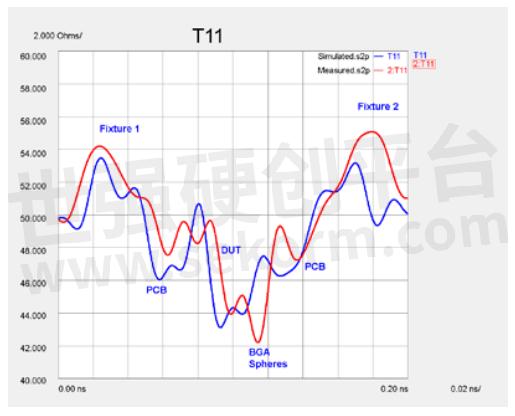
Figure 4: A single-ended TDR plot.
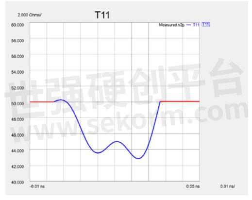
Figure 5: The original TDR measurement without the PCB and BGA used in the standard characterization method to produce the specification data.
In conclusion, socket suppliers provide specification sheets for socket and pin families to provide customers with a way of comparing one design to another. These specifications should only be considered as a reference point in making an initial decision on the preferred socket technology for an application. The customer should then provide a detailed pin-out map of their device showing the location of high-speed data lines that provide the SI engineer information necessary for further device-specific simulation. Simulation tools should always be validated by correlating the results with actual measurements to ensure confidence i n t he r e s u lt s. Traditionally, simulations have only focused on the socket without including parasitic effects caused by PCB pads and the BGA. This could set the expectation for socket performance which when included in the customer’s Spice simulation, may fall short of reality. IC manufacturers are beginning to set standards for simulations and provide the information needed to create more accurate models, which gives t h e s o cke t d e sig n e r the opportunity to optimize interfaces, as well as the entire system’s performance. When PCB pads, via transitions and BGAs, are included, the customer is given a more representative model that can be used to determine real-world effects and total system performance. As data rates continue to increase, chip and socket manufacturers will need to continue to partner closely to resolve the ever-evolving complex issues facing the industry.
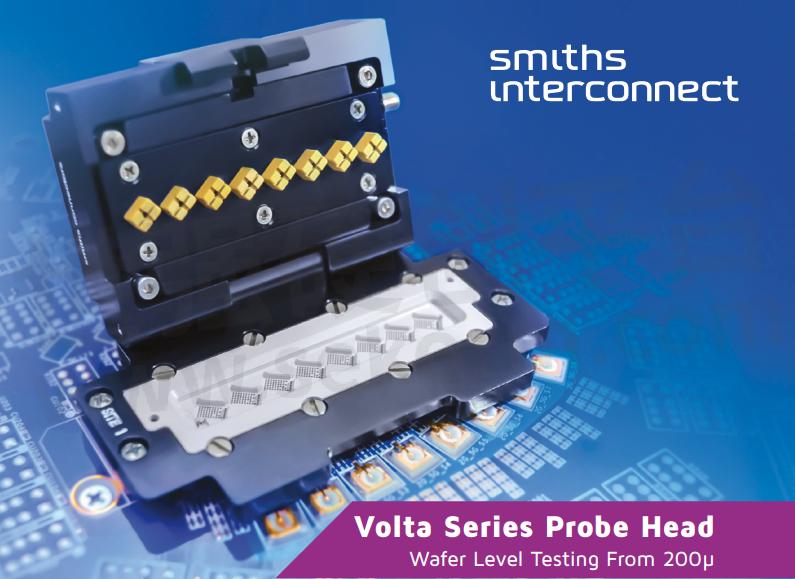
Fig.6
- +1 Like
- Add to Favorites
Recommend
- Smiths Interconnect announced the launch of its Volta 200 Series Probe Head to Enhance Wafer Test Production Efficiency
- Smiths Interconnect‘s Volta line of WLCSP Accelerating Device Brings up and Ramps up Production for WLCSP 5G Mobile ICs
- Smiths Interconnect Offered Isolators to Support NASA’s Europa Clipper Mission to Explore Jupiter’s Moon
- Smiths Interconnect’s DaVinci 112 High-Speed Test Socket Wins Best Test Measurement Award at the 2024 Global Electronics Achievement Awards
- New Volta 180 Supports Wafer Level Packages and Known Good Dies Test Businesses | Smiths Interconnect
- Smiths Interconnect Acquires Reflex Photonics to Expand in High Speed Data Transmission Market
- How Smiths Interconnect Keeps The Medical World Connected
- Smiths Interconnect Expands into Burn-In Test Market with Acquisition of Plastronics
This document is provided by Sekorm Platform for VIP exclusive service. The copyright is owned by Sekorm. Without authorization, any medias, websites or individual are not allowed to reprint. When authorizing the reprint, the link of www.sekorm.com must be indicated.
Integrated Circuits


Discrete Components


Connectors & Structural Components


Assembly UnitModules & Accessories


Power Supplies & Power Modules


Electronic Materials


Instrumentation & Test Kit


Electrical Tools & Materials


Mechatronics


Processing & Customization


