GreenPower Introduces GPL6222 Series Low Noise CMOS Voltage Regulators with Low Quiescent Current of 50μA

GreenPower's GPL6222 series low noise CMOS voltage regulator is a group of positive voltage regulators manufactured by CMOS technologies with high ripple rejection, ultra-low noise, low power consumption, and low dropout voltage, which can prolong battery life in portable electronics. The GPL6222 series works with low-ESR ceramic capacitors, reducing the amount of board space necessary for power applications. The GPL6222 series consumes less than 0.1μA in shutdown mode and has a fast turn-on time of less than 50μS. The series is very suitable for the battery-powered equipments, such as RF applications and other systems requiring a quiet voltage source.
Features
Low Quiescent Current: 50μA
High Ripple Rejection:80dB@1kHz
Operating Voltage Range: 1.8V~6.0V
Low Dropout Voltage: 60mV@100mA
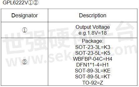
Output Voltage:1.0~ 5.0V
High Accuracy: ±2%(Typ.)
TTL-Logic-Controlled Shutdown Input
Excellent Line and Load Transient Response
Built-in Current Limiter, Short-Circuit Protection
Applications
Cellular Phones and Smart Phones
Radio control systems
Laptop, Palmtops and PDAs
Digital Still Cameras and Video Cameras
MP3 Player, MP4 Player
Battery-Powered Equipment
Order Information
Absolute Maximum Ratings (Ta=25℃,unless otherwise noted)
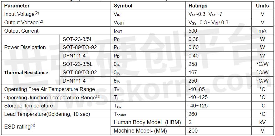
(1) Stresses beyond those listed under absolute maximum ratings may cause permanent damage to the device. These are stress ratings only, and functional operation of the device at these or any other conditions beyond those indicated under recommended operating conditions is not implied. Exposure to absolute-maximum-rated conditions for extended periods may affect device reliability.
(2)All voltages concern the network ground terminal.
(3)This IC includes overtemperature protection that is intended to protect the device during momentary overload. Junction temperature will exceed 125℃ when overtemperature protection is active. Continuous operation above the specified maximum operating junction temperature may impair device reliability.
(4)ESD testing is performed according to the respective JESD22 JEDEC standard. The human body model is a 100 pF capacitor discharged through a 1.5kΩ resistor into each pin. The machine model is a 200pF capacitor discharged directly into each pin.
Electrical Characteristics(VIN=VOUT+1V, CIN=COUT=1μF,TA=25℃, unless otherwise specified)

1) VOUT: Specified Output Voltage.
2) VOUT(E): Effective Output Voltage ( Ie. The output voltage when VIN = (VOUT +1.0V) and maintains a certain IOUT Value).
3) Vdif: The Difference Between Output Voltage And Input Voltage When Input Voltage Is Decreased Gradually Till Output Voltage Equals To 98% Of VOUT (E).
- +1 Like
- Add to Favorites
Recommend
- GreenPower 300mA CMOS Voltage Regulators GPL6232 Series with Ultra-low Power Consumption and Low Dropout Voltage
- GreenPower Introduces GPL6335 Series 18V Low Current Consumption 100mA CMOS Voltage Regulator with 2.5μA Low Quiescent Current
- GreenPower‘s GPL6331A Series Low Current Consumption 300mA CMOS Voltage Regulator Allows an Input Voltage as High as 18V
- GPL6376 Series 28V Low Current Consumption 300mA CMOS Voltage Regulator Suitable for the Battery-powered Equipments
- GPL6221 Series Low Noise CMOS Voltage Regulators with High Ripple Rejection and Low Power Consumption Less Than 0.1μA
- Bi-direction Transient Voltage Suppressors GESDBU5V0Y1 with a Low Reverse Stand−off Voltage of 5V Max and Fast response time
- GPL6109 Series Ultra Fast High PSRR Low Noise CMOS Voltage Regulators for Battery-powered Equipments
- AiT‘s A6303D: a 300mA Ultra Low Noise, 1V output CMOS LDO for Power Management Units in Portable Electronic Applications
This document is provided by Sekorm Platform for VIP exclusive service. The copyright is owned by Sekorm. Without authorization, any medias, websites or individual are not allowed to reprint. When authorizing the reprint, the link of www.sekorm.com must be indicated.
Integrated Circuits


Discrete Components


Connectors & Structural Components


Assembly UnitModules & Accessories


Power Supplies & Power Modules


Electronic Materials


Instrumentation & Test Kit


Electrical Tools & Materials


Mechatronics


Processing & Customization


