High Voltage MOS/IGBT Short Circuit Protection Circuit

High voltage MOS/IGBT Short Circuit Protection Circuit
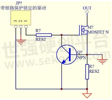
The 3-pin of the drive with short-circuit protection lock is the short-circuit signal detection end; 2 feet for driving ground; 1 pin is the drive output.

Fig.1
When there is a short circuit in the circuit, the current flowing through MOS is very large, and the voltage drop generated at both ends of the S-pole resistance causes the triode to enter the conduction from the cut-off to the conduction (of course, the conduction to the specific degree depends on the transconductance of MOS). Therefore, there is a voltage drop in the driving resistance and MOS enters the amplifier. At this time, the high voltage will not carry out strong current discharge through MOS, so the chip will not have the possibility of local overheating. In a very short time, the protection circuit detects the presence of a short circuit shuts down, and locks the drive voltage output. MOS only suffers constant current power loss within the operation time, which greatly improves its safety.
This circuit is only used to understand the principle using specific parameters to see the actual conditions selected.
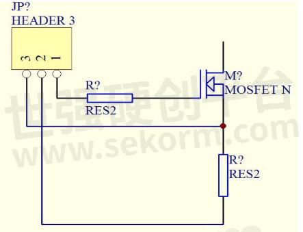
The s-class resistor is selected based on the IDM(Pulsed Drain Current allowance) of the MOS you choose. Transconductance is not the main factor. The transistor does not work in the on-off state. It only adjusts the drive voltage of MOS according to the transient current value of MOS, to ensure that the IDM will not exceed the safe working range in the case of a short circuit. At this time, the drive has been turned off and locked in 1US or even less time, so there is no power loss. The faster the reaction time of the transistor, the better. This circuit has evolved from the current negative feedback circuit. The circuit is as follows:

Fig.2
- +1 Like
- Add to Favorites
Recommend
This document is provided by Sekorm Platform for VIP exclusive service. The copyright is owned by Sekorm. Without authorization, any medias, websites or individual are not allowed to reprint. When authorizing the reprint, the link of www.sekorm.com must be indicated.


