COOLMOS Learning project

1. COOLMOS in the past
COOLMOS, also known as Super Junction MOS, has been called COOLMOS since the term Infineon is commonly used.
(Please refer to the thesis of Dr. Liu of Xi 'a Core Electronics Shanghai R&D Center and related network materials below)
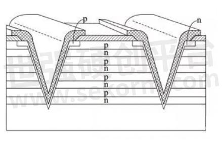
In 1988, D.J.Oe of Philips America applied for the US patent no. US Pat:4754310, and proposed for the first time that, based on LDMOS structure, pn alternate structure was adopted to replace the original single light-concentration doped drift region, and the method of effectively keeping the voltage withstand of the device while lowering the on-off resistance was used to realize the super-junction device in the real sense. As shown in Figure 1, in the original traditional LDMOS drift region, the pn alternating structure replaces the single low-concentration doped drift region, and the leakage end of LDMOS is the highly doped N + region, which is directly connected to the PN alternating drift region.

Fig.1LDMOS PN alternate structure diagram
2. Structural differences between SJ_MOS and VDMOS
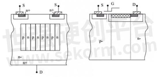
To overcome the contradiction between traditional MOS conduction resistance and breakdown voltage, some people proposed a new type of ideal device structure based on VDMOS, which is called hyperjunction MOS. The structure of hyperjunction MOS is shown in Figure 2, which consists of a series of Alternate p-type and N-type semiconductor thin layers. In the cut-off state, due to the mutually compensating effect of the depletion zone electric field in the P-type and N-type layers, the doping concentration of the P-type and N-type layers can be very high without causing the drop of the device breakdown voltage. When conducting, such a high concentration of doping can make its conducting resistance significantly decreased, about two orders of magnitude. Because of this special structure, the performance of hyperjunction MOS is better than that of traditional VDMOS. It can be seen from the following table that the parameters of hyperjunction MOS of SMIC electron are better than those of planar MOS.

Fig.2 Schematic diagram of composite buffer layer structure
For conventional VDMOS device structure, the contradictory relationship between Rdson and BV should be improved by reducing EPI parameter concentration. However, the epitaxial layer is a channel for forward current flow. When EPI parameter concentration is reduced, the resistance must be increased and Rdson will be increased. Rdson directly determines the loss of the MOSFET monomer. Therefore, for ordinary VDMOS, the contradiction between the two is irreconcilable, which is the limitation of conventional VDMOS.
But with hyperjunction MOS, the contradiction is less obvious. By setting a P zone deep into the EPI, the BV is greatly improved without affecting Rdson. For conventional VDMOS, the reverse withstand voltage is mainly dependent on the PN junction between n-type EPI and body area; for a PN junction, the withstand voltage is mainly dependent on the depletion zone bearing, the size of the electric field in the depletion zone, and the area of the expansion width of the depletion zone. In conventional VDSMO, P body concentration is greater than N EPI, it should also be clear, the p-n junction depletion region mainly to the low diffusion mixed side, so this structure, the P side body area, depletion region extension is very small, basic has little contribution to pressure, pressure mainly P body - N EPI area in the side of the N type, the area of electric field intensity is a gradual change, the closer to the surface of a p-n junction, the greater the electric field intensity E. The COOLMOS structure, due to set up a relatively lower P P body concentration region area, so the P area on the side of the depletion region will greatly expand, and this area is deep in the EPI, causing the p-n junction can bear large voltage on both sides, in other words, is the peak electric field Ec by near the device surface, in areas where the device internal deeply moved.

Fig.3 Tihanyi patent hyperjunction schematic diagram
- +1 Like
- Add to Favorites
Recommend
- Laird Thermal Systems Launches the SuperCool X Series with Next-Gen Thermoelectric Cooling Technology
- High-performance Thermoelectric Coolers Offer A Flexible Active Cooling Option for Spot Cooling of Lidar Sensors
- Data Center Installations: In-Rack Cooling or In-Row Cooling?
- Air Cooled VCSEL Applications with Rogers Micro-Channel-Coolers (MCC)
- Laird Thermal Systems Offers Thermoelectric Coolers, Thermoelectric Cooler Assemblies and Temperature Controllers for Refrigerated Centrifuges
- JOHNSON ELECTRIC‘s VOLTA High Voltage Cooling Fan Module: Breakthrough in Powertrain Cooling Technology Driving the Future of Efficient Automotive Cooling
- Laird Thermal Systems OffersThermoelectric Coolers and Assemblies for Medical Applications
- Hi-semicon‘s 3A/500V N-Channel Enhancement Mode Power MOSFET SFF3N50TS and SFD3N50TS
This document is provided by Sekorm Platform for VIP exclusive service. The copyright is owned by Sekorm. Without authorization, any medias, websites or individual are not allowed to reprint. When authorizing the reprint, the link of www.sekorm.com must be indicated.


